Vertical NPNP Structure In a Triple Well CMOS Process

a triple well, cmos technology, applied in the direction of semiconductor/solid-state device details, instruments, transistors, etc., can solve the problems of complex esd protection in mixed signal applications, large damage to currents within integrated circuits, and the need for analog signals to be handled

Inactive Publication Date: 2012-05-24
ALSEPHINA INNOVATIONS INC
View PDF1 Cites 12 Cited by
  • Summary
  • Abstract
  • Description
  • Claims
  • Application Information

AI Technical Summary

Problems solved by technology

Chips are often exposed to electrostatic discharge (ESD) events leading to potentially large and damaging currents within the integrated circuit.
The problem of providing effective ESD protection in mixed signal applications is further complicated by the necessity of handling analog signals.

Method used


Image

  • Vertical NPNP Structure In a Triple Well CMOS Process
  • Vertical NPNP Structure In a Triple Well CMOS Process
  • Vertical NPNP Structure In a Triple Well CMOS Process

Examples


Embodiment Construction

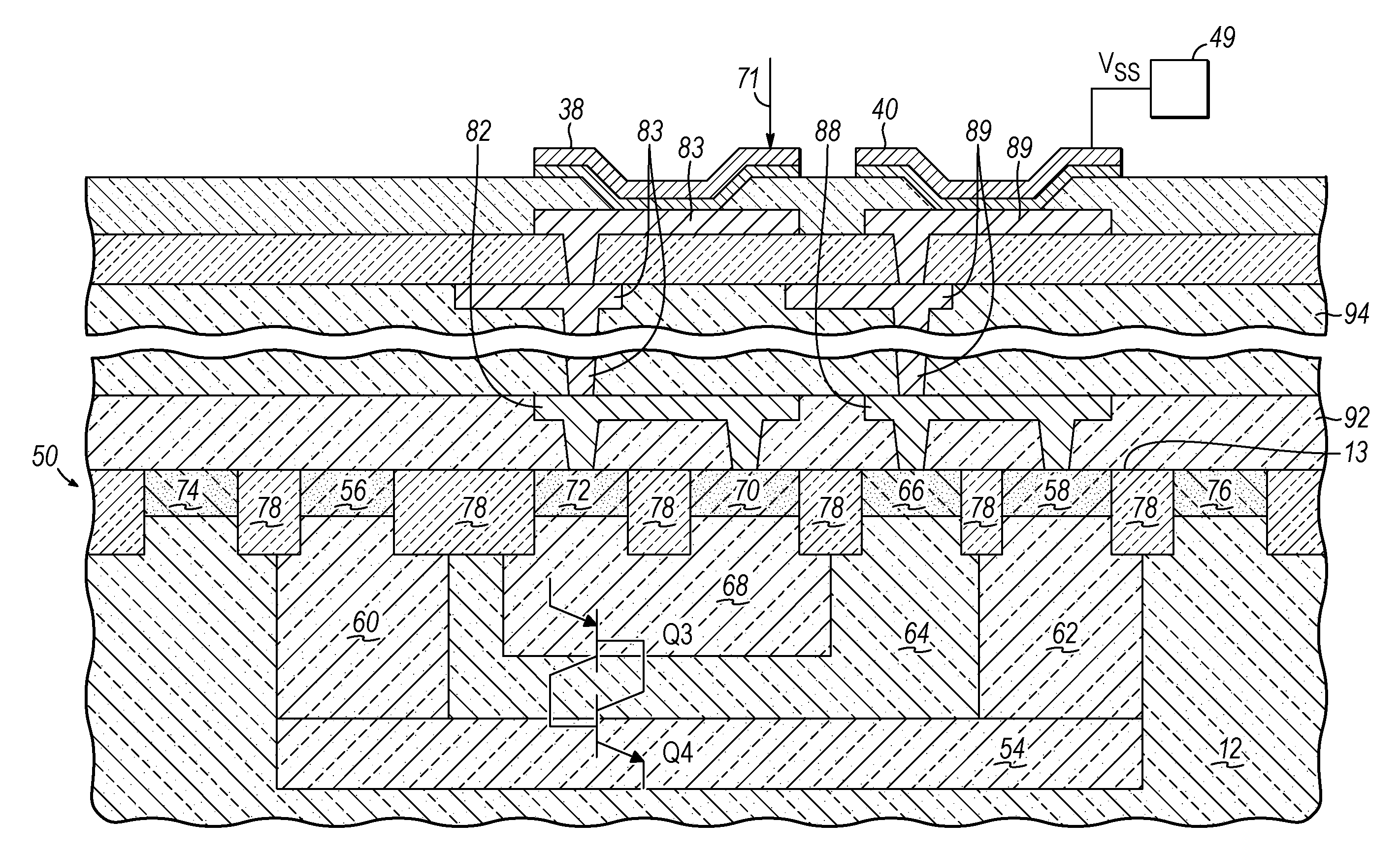
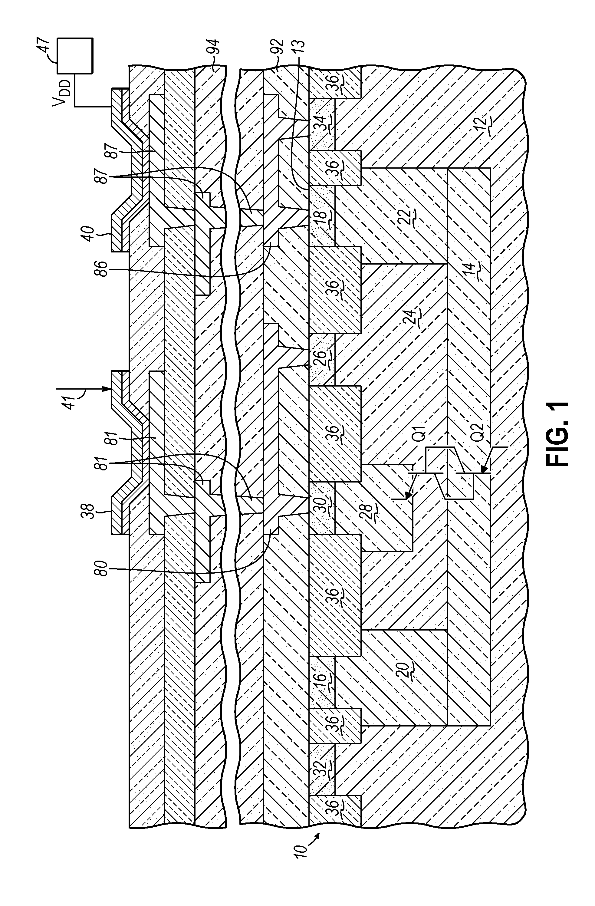
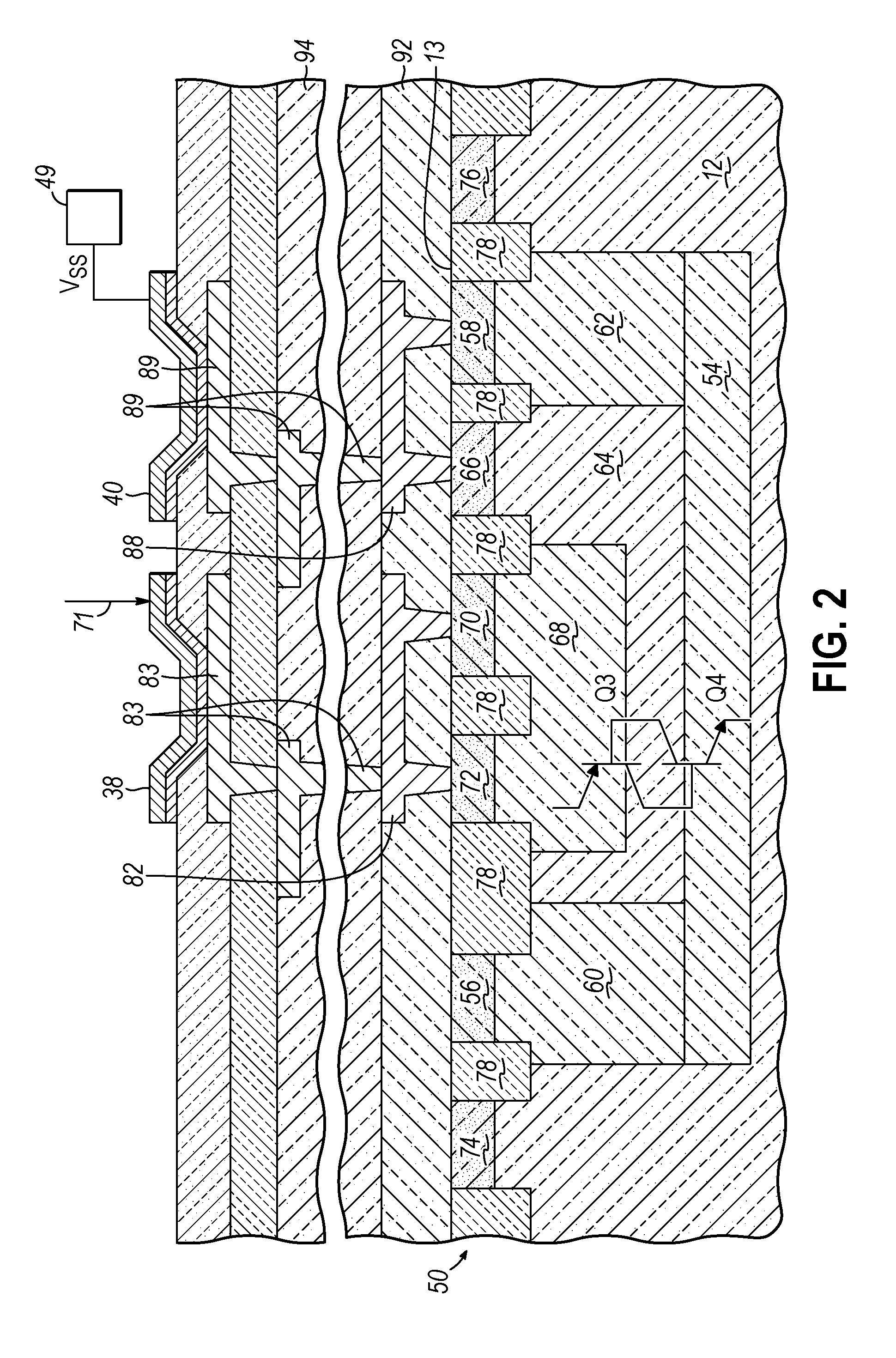
[0014]A triple well process is typically implemented in CMOS and BiCMOS processes to improve isolation between devices. In a typical single well process implemented on a p-type substrate, islands of n-type silicon (n-wells) may be established within a p-type substrate as a step in forming CMOS devices. Additional wells may then be formed within the n-wells by introducing p-type dopants in a concentration effective to form p-wells when activated. A triple well process may establish additional n-doped wells within a p-well to form a series of alternately doped semiconductor islands, which allows later formed islands to be enclosed by earlier formed islands. Devices may thereby be isolated from each other by the depletion regions that form near the boundaries between n-type and p-type semiconductors. In particular, the depletion layer between the p-type substrate and the first n-well may provide isolation between the substrate and devices formed in the n-well. Similar structures may al...


PUM


Abstract

A vertical NPNP structure fabricated using a triple well CMOS process, as well as methods of making the vertical NPNP structure, methods of providing electrostatic discharge (ESD) protection, and design structures for a BiCMOS integrated circuit. The vertical NPNP structure may be used to provide on-chip protection to an input/output (I/O) pad from negative-voltage ESD events. A vertical PNPN structure may be also used to protect the same I/O pad from positive-voltage ESD events.

Description

BACKGROUND[0001]The present invention relates generally to semiconductor device fabrication and, more particularly, to electrostatic discharge (ESD) devices for protecting an Input / Output pad in radio frequency and analog mixed signal applications, as well as methods of forming ESD protection devices and design structures for BiCMOS integrated circuits.[0002]Modern electronics achieve high levels of functionality in small form factors by integrating multiple functions onto a single chip. A common fabrication process that allows high levels of integration at a relatively low cost is Complementary Metal-Oxide-Semiconductor (CMOS). CMOS processes build a combination of p-type and n-type metal-oxide-semiconductor field-effect transistors (MOSFETs) to implement logic gates and other types of digital circuits. By introducing additional fabrication steps into a CMOS process forming MOSFETs, bipolar junction transistors can also be formed in a process commonly known as BiCMOS. BiCMOS proces...

Claims


Application Information

Patent Timeline
Patent Type & Authority Applications(United States)
IPC IPC(8): H01L29/74G06F17/50H01L21/332
CPCH01L21/823892H01L27/0262H01L27/0928H01L29/74H01L2924/0002H01L2924/00
Inventor CAMPI, JR., JOHN B.CHANG, SHUNHUA T.CHATTY, KIRAN V.GAUTHIER, JR., ROBERT J.LI, JUNJUNMISHRA, RAHULMUHAMMAD, MUJAHID
Owner ALSEPHINA INNOVATIONS INC
Why Eureka
Try Eureka