Vertical Semiconductor Device with Thinned Substrate
a technology of semiconductor devices and substrates, applied in semiconductor devices, semiconductor/solid-state device details, electrical devices, etc., can solve the problems of limiting the performance of ideal power devices, consuming a large amount of area, and dissipating a large amount of hea
- Summary
- Abstract
- Description
- Claims
- Application Information
AI Technical Summary
Problems solved by technology
Method used
Image

Examples
Embodiment Construction
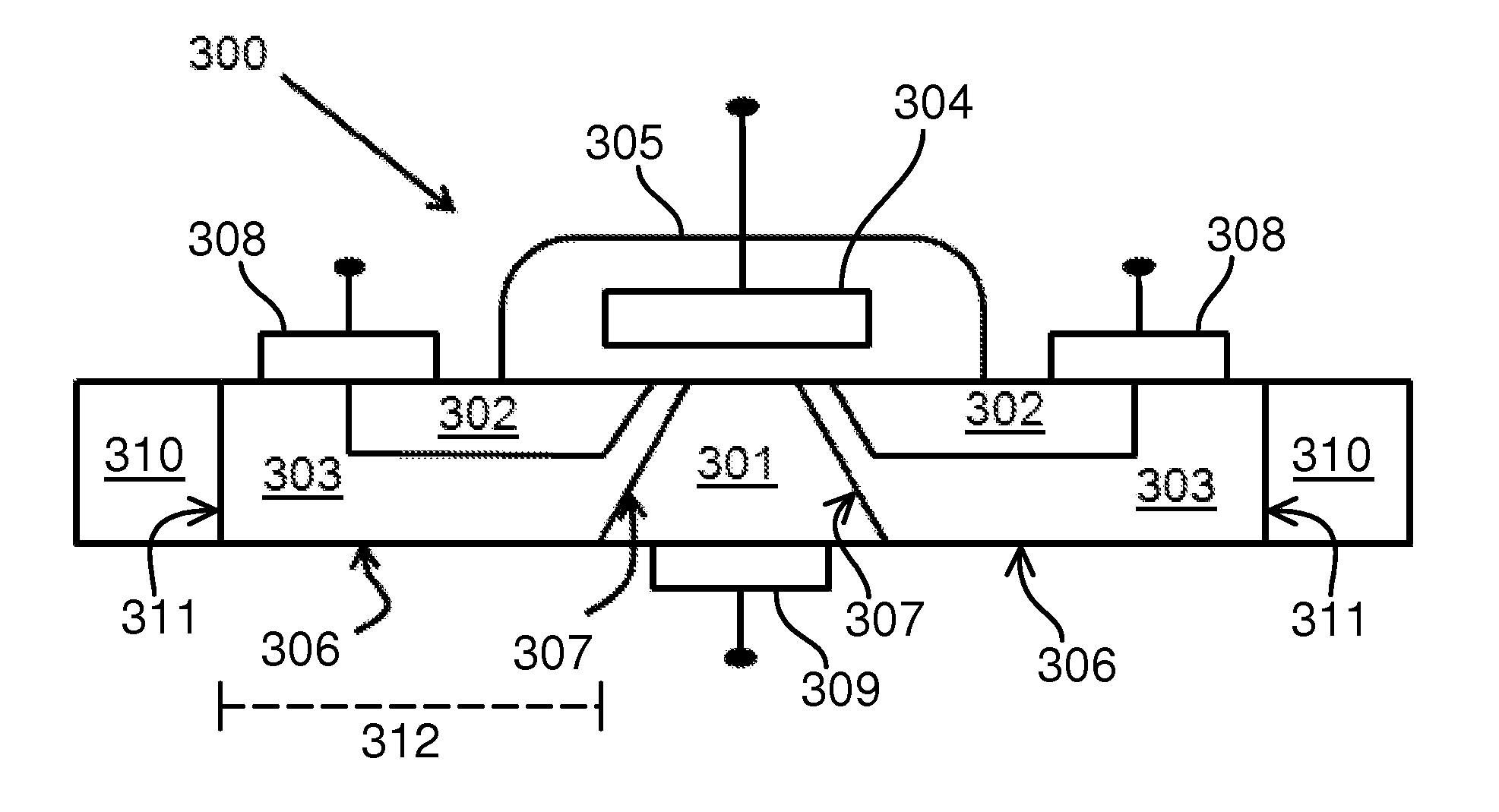
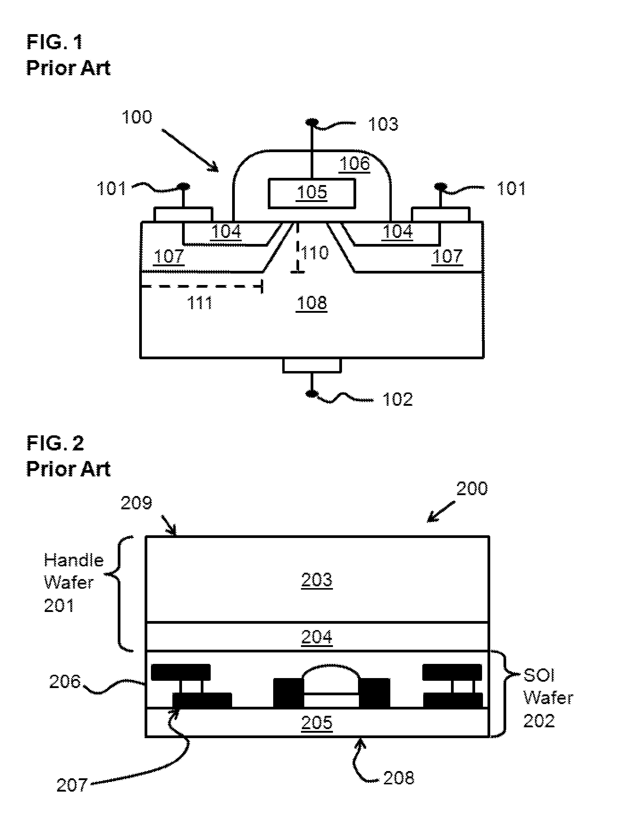
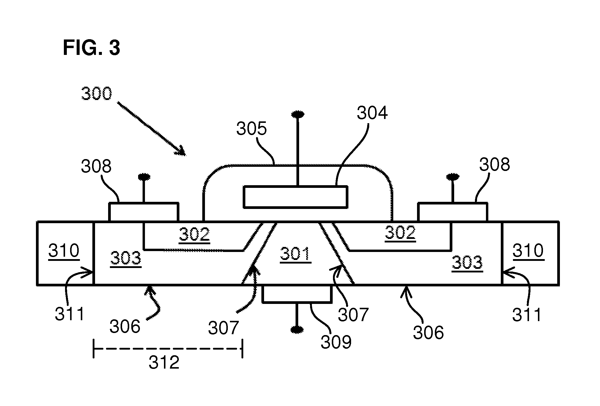
[0030]The present invention is illustrated in several related example embodiments described below. Each embodiment generally exhibits improvements in the performance metrics described in the background, e.g. electrical performance improvements in the ability to transition rapidly from an off state to an on state and thermal performance improvements in the ability to dissipate large amounts of heat. In addition, some of the embodiments enable additional benefits from the ability to independently bias the source and body of a power transistor. Additionally, some of the embodiments achieve some of the improvements or benefits by including layer transfer structures and techniques. Furthermore, some of the improvements or benefits are enabled by thinning the semiconductor substrate, whether using an SOI (semiconductor on insulator) or bulk semiconductor wafer, and with or without layer transfer structures and techniques. Also, some embodiments achieve some improvements by including an is...
PUM
 Abstract
Description
Claims
Application Information
 - R&D
- Intellectual Property
- Life Sciences
- Materials
- Tech Scout
- Unparalleled Data Quality
- Higher Quality Content
- 60% Fewer Hallucinations
Browse by: Latest US Patents, China's latest patents, Technical Efficacy Thesaurus, Application Domain, Technology Topic, Popular Technical Reports.
© 2025 PatSnap. All rights reserved.Legal|Privacy policy|Modern Slavery Act Transparency Statement|Sitemap|About US| Contact US: help@patsnap.com