


Quick Research
Generate reliable direction feasibility study reports for your R&D in just a few steps.

Technical Q&A
Discover and master advanced knowledge NOW. Basics, ideas, possibilities, all at once.

Find Solutions
As an expert in R&D theories, this can generate solutions to your technical problems instantly.

Evaluate Feasibility
Analyze your overall solution with one click, know your potential R&D risks in advance.

Monitor Landscape
Get weekly tech updates, stay abreast of the latest tech innovations and key insights.
Switchable memory diodes based on ferroelectric/conjugated polymer heterostructures and/or their composites
a memory diode and ferroelectric/conjugated polymer technology, applied in the field of memory cells, can solve the problems of increasing costs, slowing down the speed of volatile memory cells, and losing information
- Summary
- Abstract
- Description
- Claims
- Application Information
AI Technical Summary
Benefits of technology
Problems solved by technology
Method used
Image

Examples
second embodiment
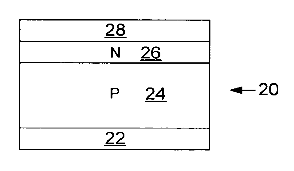
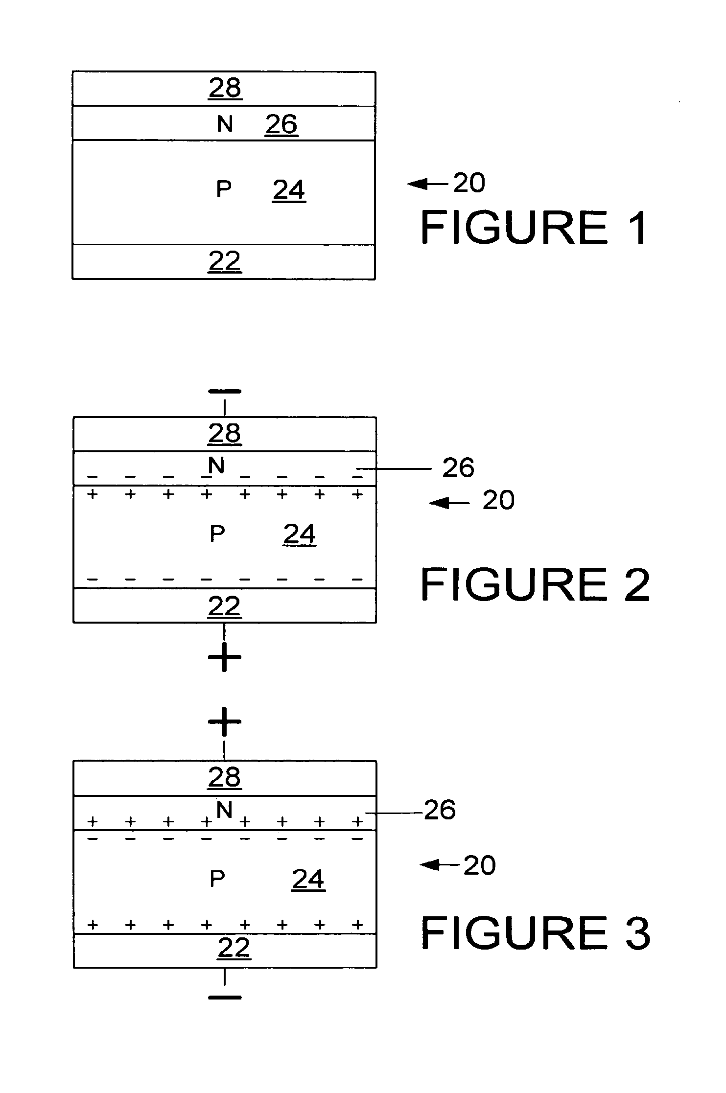
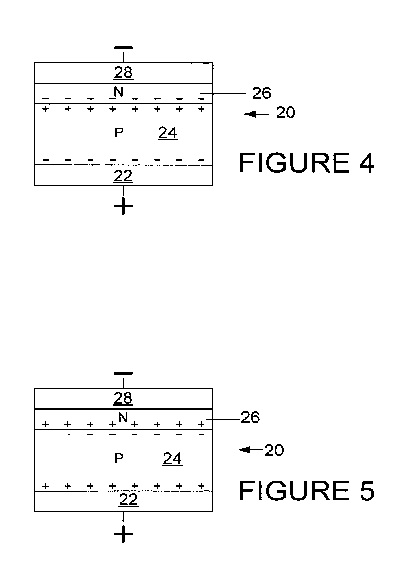
[0038]FIGS. 8 and 9 illustrate the invention. As such, the memory cell 40 includes electrodes 42, 48 and layer 44 of p type ferroelectric semiconductor material as described above, but now includes a layer 46 of n type semiconductor material such as doped silicon, germanium, tin oxide, or metal dichalcogenides (MX2: M=Mo, W; X=S, Se) in place of the conjugated semiconductor polymer layer. In the programming procedure (FIG. 8), again, a positive voltage is applied to the electrode 42, while a negative voltage is applied to the electrode 48, so that an electrical potential (Vpg) is applied across the cell 20 from higher to lower potential in the direction from the electrode 42 to the electrode 48. In accordance with the ferroelectric properties of the layer 44, positive charge will be generated within the layer 44 near the surface of the layer 44 adjacent the semiconductor layer 46, while negative charge will be generated within the layer 44 near the surface of the layer 44 adjacent t...
third embodiment
[0041]FIGS. 10 and 11 illustrate the invention. As such, the memory cell 50 includes electrodes 52, 58 and p type layer 54 of ferroelectric semiconductor material as described above with respect to FIGS. 1-5, but now includes another p type layer 56 of ferroelectric semiconductor material in place of the conjugated polymer layer, but with the ferroelectric semiconductor material of the layer 56 having a switching potential which is different from the switching potential of the ferroelectric semiconductor material of the layer 54 (achieved by providing different doping characteristics of the layers 54, 56). In this particular example, the switching potential of the layer 56 is lower than the switching potential of the layer 54, i.e., layer 56 requires a lower potential for switching its state than layer 54.
[0042]In the programming procedure (FIG. 10), again, a positive voltage is applied to the electrode 52, while a negative voltage is applied to the electrode 58, so that an electric...
fourth embodiment
[0045]FIGS. 12 and 13 illustrate the invention. As such, the memory cell 60 includes electrodes 62, 66, but now includes only a layer 64 therebetween which is a composite of ferroelectric semiconductor material as described above and a conjugated polymer.
[0046]In the programming procedure (FIG. 12), again, a positive voltage is applied to the electrode 62, while a negative voltage is applied to the electrode 66, so that an electrical potential (Vpg) is applied across the cell 60 from higher to lower potential in the direction from the electrode 62 to the electrode 66. This electrical potential causes the layer 64 to switch to the state shown in FIG. 12.
[0047]In the erasing procedure (FIG. 13), a positive voltage is applied to the electrode 66, while a negative voltage is applied to the electrode 62, so that an electrical potential (Ver) is applied across the cell 60 from higher to lower potential in the direction from the electrode 66 to the electrode 62. This electrical potential c...
PUM
 Abstract
Description
Claims
Application Information
 - R&D Engineer
- R&D Manager
- IP Professional
- Industry Leading Data Capabilities
- Powerful AI technology
- Patent DNA Extraction
Browse by: Latest US Patents, China's latest patents, Technical Efficacy Thesaurus, Application Domain, Technology Topic, Popular Technical Reports.
© 2024 PatSnap. All rights reserved.Legal|Privacy policy|Modern Slavery Act Transparency Statement|Sitemap|About US| Contact US: help@patsnap.com