


Quick Research
Generate reliable direction feasibility study reports for your R&D in just a few steps.

Technical Q&A
Discover and master advanced knowledge NOW. Basics, ideas, possibilities, all at once.

Find Solutions
As an expert in R&D theories, this can generate solutions to your technical problems instantly.

Evaluate Feasibility
Analyze your overall solution with one click, know your potential R&D risks in advance.

Monitor Landscape
Get weekly tech updates, stay abreast of the latest tech innovations and key insights.
Ferroelectric semiconductor memory device
a technology of ferroelectric memory and semiconductors, which is applied in the direction of information storage, static storage, digital storage, etc., can solve the problems of affecting the speed of writing, the potential of the plate line is long, and the time required to write information to the ferroelectric memory cell is long
- Summary
- Abstract
- Description
- Claims
- Application Information
AI Technical Summary
Benefits of technology
Problems solved by technology
Method used
Image

Examples
first embodiment
[0023]An embodiment of the present invention is described below.
[0024]This embodiment relates to methods of erasing and writing information to a TC parallel unit series-connected ferroelectric memory, which is a ferroelectric memory.
[Entire Configuration of Ferroelectric Memory Cell]
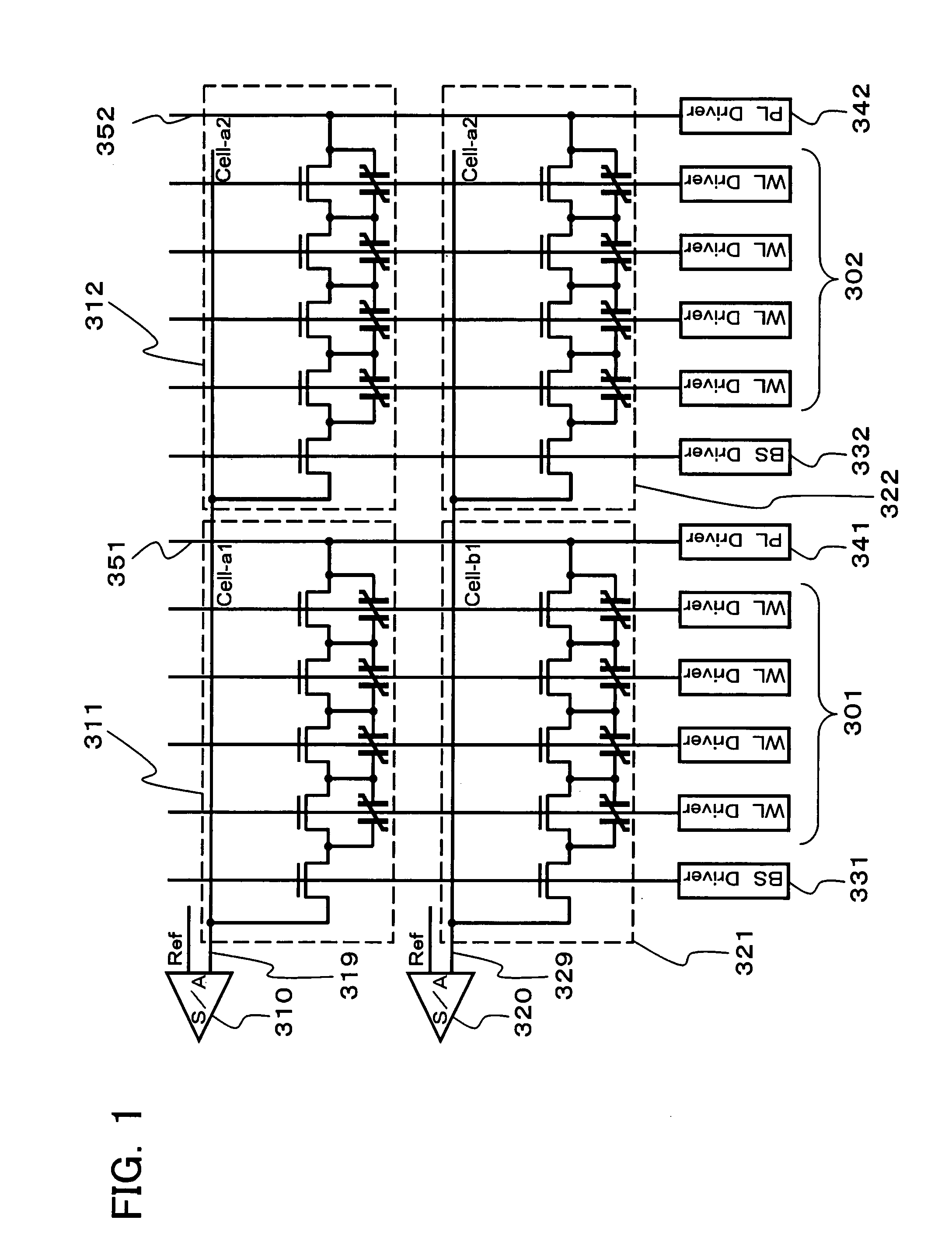
[0025]FIG. 1 shows a configuration of a ferroelectric memory cell array in this embodiment. Referring to FIG. 1, the memory cell array includes cell units 311, 312, 321, and 322 arranged two-dimensionally. Each cell unit includes a memory cell block and a selection transistor connected to one end of the block. The block includes a plurality of ferroelectric memory cells connected in series. Each memory cell includes a ferroelectric capacitor and a transistor connected thereto. A set of cell units arrayed along the lateral direction in FIG. 1 connects to a common bit line 319. Another set of cell units in the lateral direction connects to a common bit line 329. The bit lines 319 and 329 connect to corresp...
second embodiment
[0102]This embodiment relates to a method of reading information from the TC parallel unit series-connected ferroelectric memory, which is a ferroelectric memory. The entire configuration is similar to that in the first embodiment.
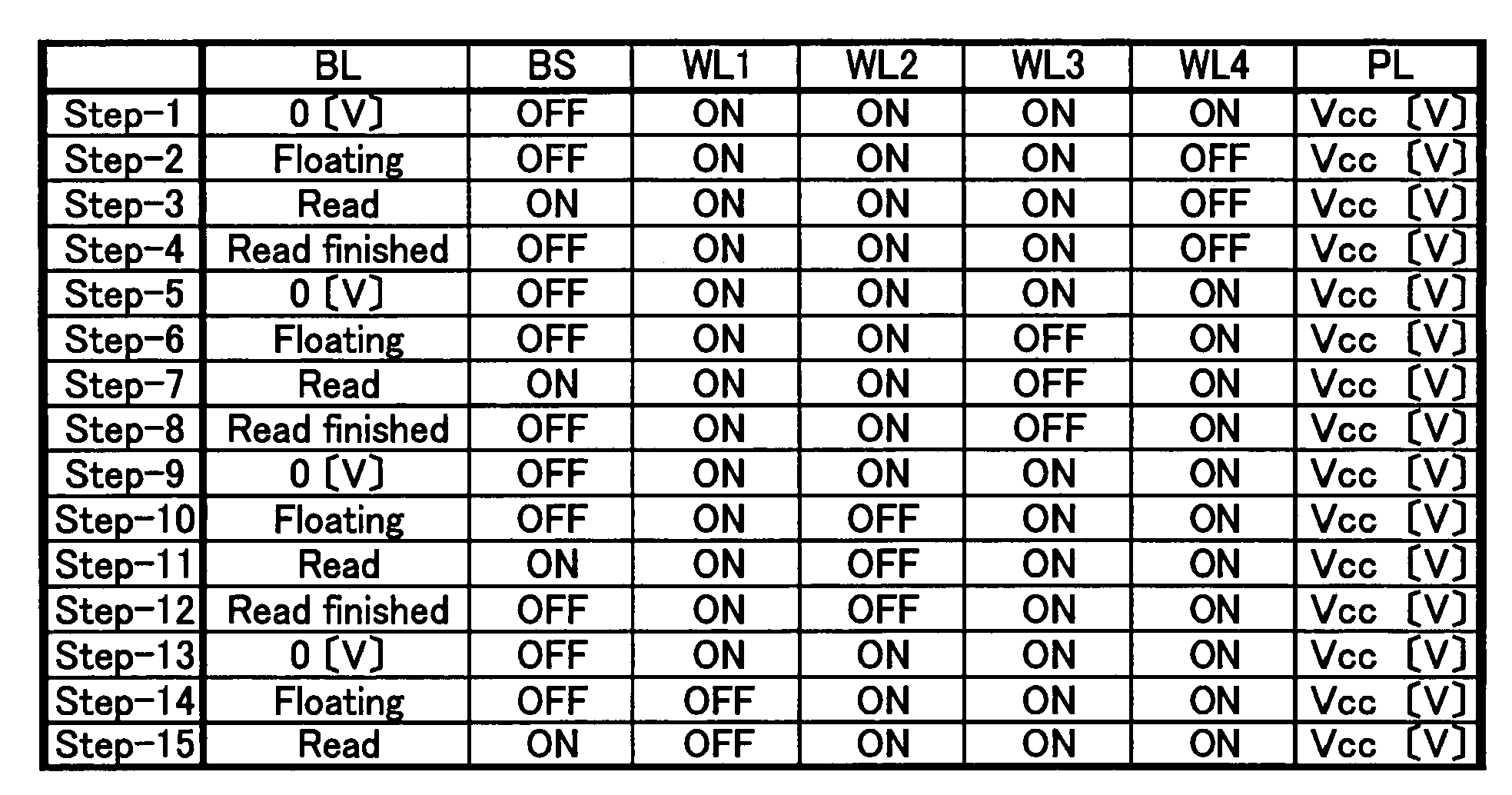
[0103]FIG. 7 shows a configuration of the block in the TC parallel unit series-connected ferroelectric memory, which is a ferroelectric memory, used in this embodiment. Referring to FIG. 7, the block has a configuration similar to that in the first embodiment. Referring to FIG. 8, a method of reading a ferroelectric memory cell in a block 101 is described below. A plate line (PL) 142 is connected to the block 101 to be read. A plate line (PL) 242 is connected to the other blocks such as a block 201. With the plate line 142 being applied with a voltage of Vcc [V] and the plate line (PL) 242 being applied with 0 [V], the reading is started.
[0104]First at Step-1, the selection transistor 111 is turned off. The word lines WL1, WL2, WL3, and WL4 are applied wit...
PUM
 Abstract
Description
Claims
Application Information
 - R&D Engineer
- R&D Manager
- IP Professional
- Industry Leading Data Capabilities
- Powerful AI technology
- Patent DNA Extraction
Browse by: Latest US Patents, China's latest patents, Technical Efficacy Thesaurus, Application Domain, Technology Topic, Popular Technical Reports.
© 2024 PatSnap. All rights reserved.Legal|Privacy policy|Modern Slavery Act Transparency Statement|Sitemap|About US| Contact US: help@patsnap.com