Method for preparing low-bandgap ferroelectric photovoltaic thin films by pulsed laser deposition
A pulsed laser deposition, ferroelectric photovoltaic technology, applied in photovoltaic power generation, circuits, electrical components and other directions, to achieve the effect of less raw materials, convenient operation and simple preparation process
- Summary
- Abstract
- Description
- Claims
- Application Information
AI Technical Summary
Problems solved by technology
Method used
Image
Examples
Embodiment 1
[0022] Using Pt / Ti / SiO 2 / Si(100) as the substrate, cleaned with acetone, absolute ethanol, and deionized water for 10 minutes in an ultrasonic cleaner with a working frequency of 40kHz, then dried with nitrogen and immediately placed in a vacuum chamber. Set the distance between the target stage and the sample stage to be 30mm, the substrate temperature to be 600°C, the oxygen pressure in the vacuum chamber to be 0Pa, the laser pulse energy to be 100mJ, the pulse laser frequency to be 1Hz, and the rotation speeds of the sample stage and the target stage to be 10r / min and Under the conditions of 5r / min and deposition time of 10 minutes, a low bandgap (KNbO 3 ) 0.9 (BaNi 0.5 Nb 0.5 o 3 ) 0.1 (KBNNO) Ferroelectric photovoltaic thin films.
Embodiment 2
[0024] Using Pt / Ti / SiO 2 / Si(100) was used as the substrate, cleaned with acetone, absolute ethanol, and deionized water for 10 minutes in an ultrasonic cleaner, and the operating frequency of the ultrasonic cleaner was 40kHz, then dried with nitrogen and immediately placed in a vacuum chamber. Set the distance between the target stage and the sample stage to be 30mm, the substrate temperature to be 700°C, the oxygen pressure in the vacuum chamber to be 0.01Pa, the laser pulse energy to be 100mJ, the pulse laser frequency to be 5Hz, and the rotation speed of the sample stage and the target stage to be 10r / min respectively And 5r / min, deposited for 20 minutes, prepared a low band gap (KNbO 3 ) 0.9 (BaNi 0.5 Nb 0.5 o 3 ) 0.1 (KBNNO) Ferroelectric photovoltaic thin films.
Embodiment 3
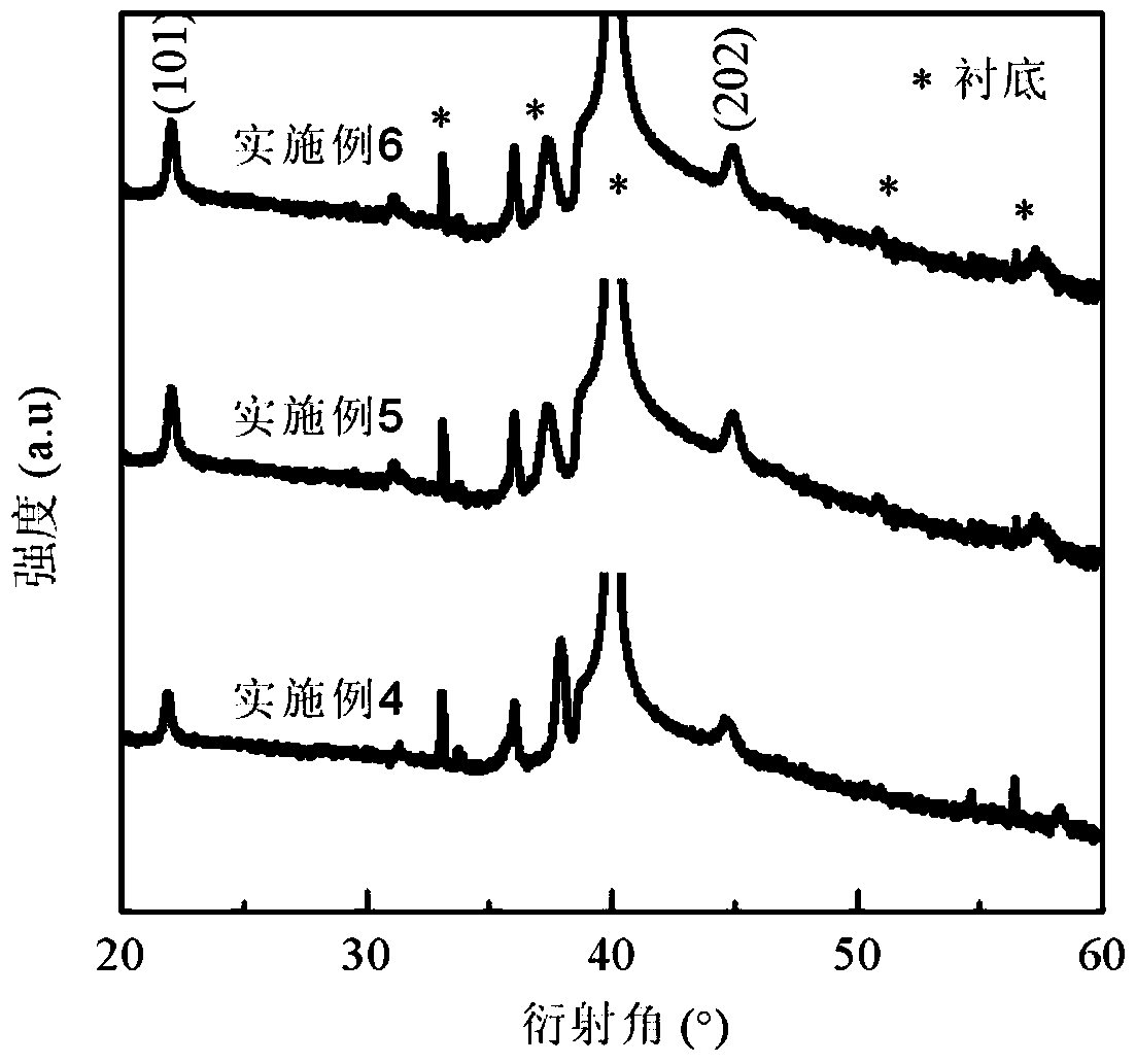
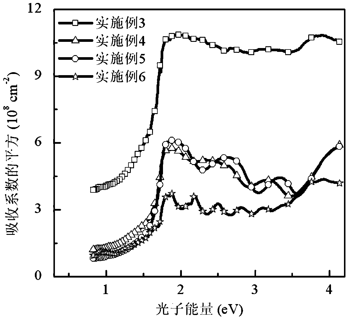
[0026] Using Pt / Ti / SiO 2 / Si(100) was used as the substrate, cleaned with acetone, absolute ethanol, and deionized water for 10 minutes in an ultrasonic cleaner, and the operating frequency of the ultrasonic cleaner was 40kHz, then dried with nitrogen and immediately placed in a vacuum chamber. Set the distance between the target stage and the sample stage to be 55 mm, the substrate temperature to be 700 °C, the oxygen pressure in the vacuum chamber to be 0 Pa, the laser pulse energy to be 300 mJ, the pulse laser frequency to be 5 Hz, and the rotation speeds of the sample stage and the target stage to be 10 r / min and Under the conditions of 5r / min and deposition time of 20 minutes, (KNbO 3 ) 0.9 (BaNi 0.5 Nb 0.5 o3 ) 0.1 (KBNNO) Ferroelectric photovoltaic thin films. figure 2 The relationship between the absorption coefficient of the film and the incident photon energy is shown, from which it can be known that the band gap (band gap) of the KBNNO film is about 1.4eV, whi...
PUM
| Property | Measurement | Unit |
|---|---|---|
| band gap | aaaaa | aaaaa |
Abstract
Description
Claims
Application Information
 - R&D Engineer
- R&D Manager
- IP Professional
- Industry Leading Data Capabilities
- Powerful AI technology
- Patent DNA Extraction
Browse by: Latest US Patents, China's latest patents, Technical Efficacy Thesaurus, Application Domain, Technology Topic, Popular Technical Reports.
© 2024 PatSnap. All rights reserved.Legal|Privacy policy|Modern Slavery Act Transparency Statement|Sitemap|About US| Contact US: help@patsnap.com


