
System and method of selective optical pattern enhancement for semiconductor manufacturing

Active Publication Date: 2011-09-08
SEMICON MFG INT (SHANGHAI) CORP
View PDF2 Cites 2 Cited by
  • Summary
  • Abstract
  • Description
  • Claims
  • Application Information

AI Technical Summary

Benefits of technology

[0013]It is to be appreciated that embodiments of the present invention provide many advantages over conventional techniques. According to various embodiments, OPC and / or RET processes are performed on selected areas and / or structures of reticle patterns, instead being applied to the entireties of the reticle patterns. As a result, the amount of process time is reduced and the workflow is simplified. In certain embodiments, techniques according to the present invention are compatible with existing systems. For example, various processes according to embodiments of the present invention for selective OPC and / or RET are implemented as software added on to the existing reticle pattern software. There are other benefits as well.

Problems solved by technology

An IC fabrication facility can cost hundreds of millions, or even billions, of dollars.
Making devices smaller is very challenging, as each process used in IC fabrication has a limit.
Various process limitations have made IC fabrication more difficult as the devices get smaller.
This causes the projected image to exhibit some rounding and other optical distortion.
Furthermore, resist processing effects during the bake process, such as nonlinear diffusion of the photo-generated acid, exacerbate the pattern distortion on the wafer.
Subsequent pattern transfer processing effects, such as etch bias, further degrade the pattern fidelity.
While such effects pose relatively little problem in layouts with large feature sizes (e.g., layouts with critical dimensions above about 1 micron), they cannot be ignored in layouts having feature sizes smaller than about 1 micron.
The problems become especially pronounced in IC designs having feature sizes near the wavelength of light used in the photolithographic process.

Method used


Image

  • System and method of selective optical pattern enhancement for semiconductor manufacturing
  • System and method of selective optical pattern enhancement for semiconductor manufacturing
  • System and method of selective optical pattern enhancement for semiconductor manufacturing

Examples


Embodiment Construction

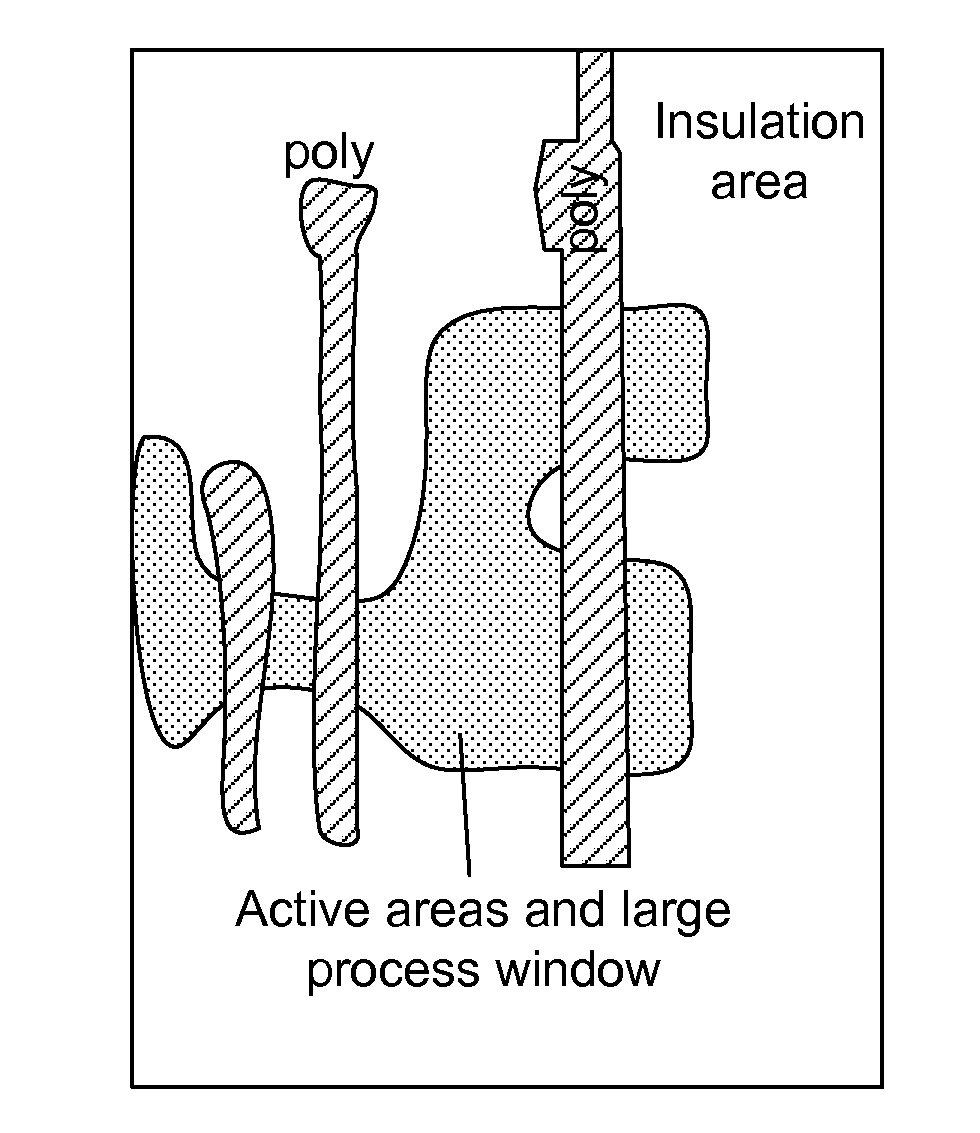
[0026]Embodiments of the present invention relate to a semiconductor processing for the manufacture of semiconductor devices. More particularly, embodiments of the present invention provide a method and device for generating suppress bars and selective optical proximity correction for the manufacture of integrated circuits.

[0027]As mentioned above, performing OPC on reticle patterns is time consuming and requires huge amount of computer resources. For example, reticle patterns are usually stored as large-size files. To perform OPC and / or a reticle pattern or design, a machine (e.g., a dedicated computer) is required to process the entirety of the reticle pattern. This process typically takes a very long time to complete.

[0028]Therefore, it is appreciated that embodiments of the present inventions provide new and improved system and methods for performing OPC and RET processes in a more efficient manner. More specifically, portions of reticle patterns are identified for the purpose o...


PUM


Abstract

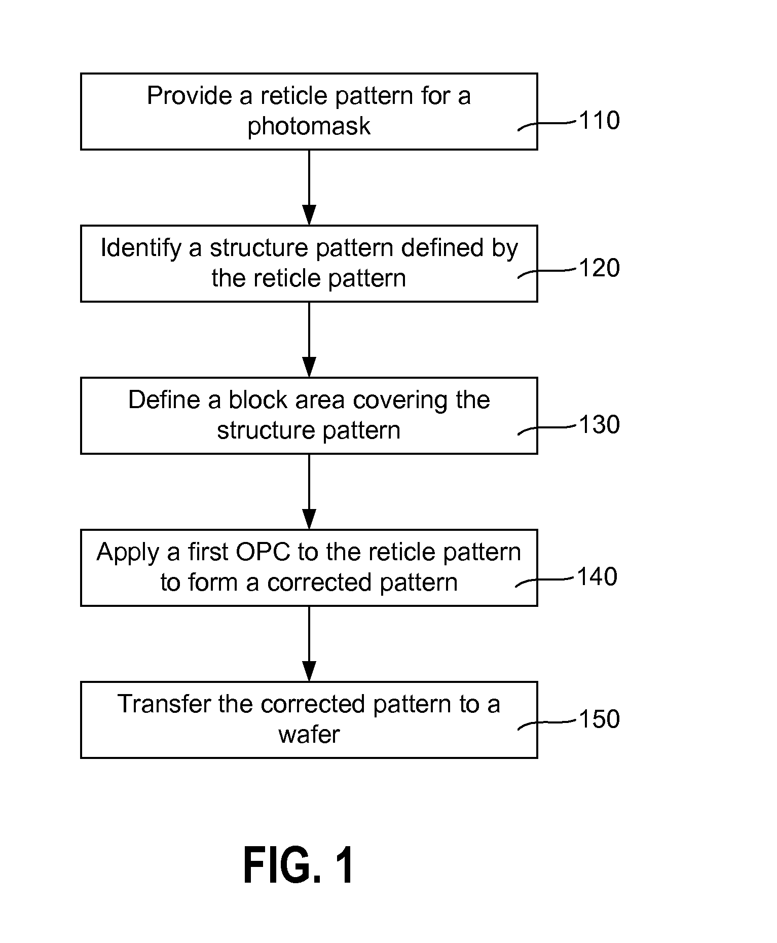
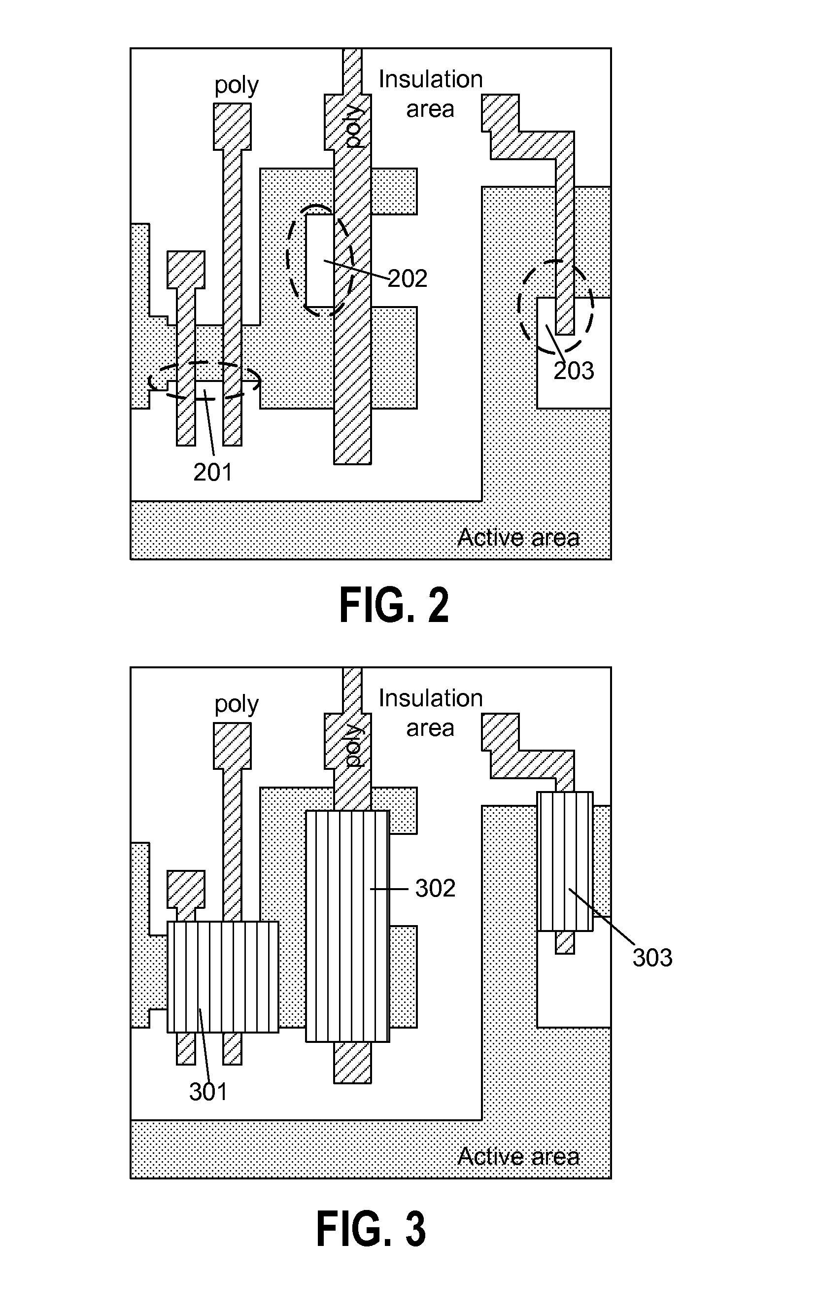
System and method of selective optical pattern enhancement for semiconductor manufacturing. A method for performing a photolithography process includes providing a reticle pattern for a photomask, the reticle pattern including one or more active areas, the photomask including at least a first active area and a first insulation area. The method also includes identifying a first structure pattern defined by the reticle pattern. Additionally, the method includes defining a block area covering the first structure, the block area being positioned within the active area. The method further includes applying at least a first optical proximity correction to the reticle pattern to form a corrected pattern, the first optical proximity correction being restricted to the block area. Also, the method includes transferring the corrected pattern to a wafer.

Description

CROSS-REFERENCES TO RELATED APPLICATIONS[0001]This application claims priority to Chinese Patent Application No. 201010118841.4, filed Mar. 5, 2010, which is commonly owned and incorporated by reference herein for all purposes.BACKGROUND OF THE INVENTION[0002]Embodiments of the present invention relate to a semiconductor processing for the manufacture of semiconductor devices. More particularly, embodiments of the present invention provide a method and device for generating suppress bars and selective optical proximity correction for the manufacture of integrated circuits.[0003]Integrated circuits or “ICs” have evolved from a handful of interconnected devices fabricated on a single chip of silicon to millions of devices. Current ICs provide performance and complexity far beyond what was originally imagined. In order to achieve improvements in complexity and circuit density (i.e., the number of devices capable of being packed onto a given chip area), the size of the smallest device f...

Claims


Application Information

Patent Timeline
IPC IPC(8): G03F7/20
CPCG03F7/20G03F1/36G03F1/70G03F7/70441
Inventor HUNG, CHI YUAN
Owner SEMICON MFG INT (SHANGHAI) CORP
Learn More