Photoelectric conversion device, imaging device, method for manufacturing imaging device, and imaging apparatus
- Summary
- Abstract
- Description
- Claims
- Application Information
AI Technical Summary
Benefits of technology
Problems solved by technology
Method used
Image

Examples
example 1
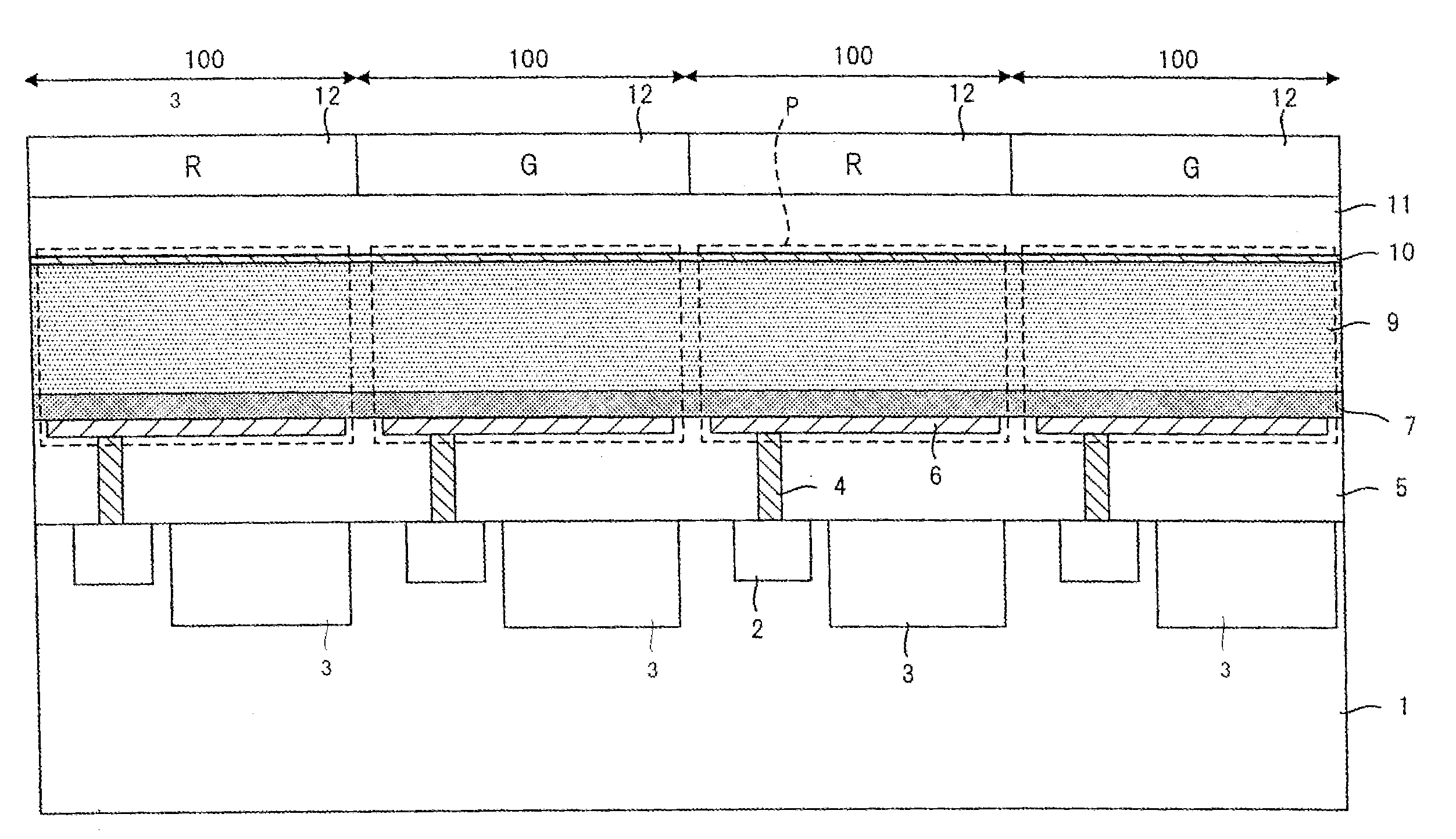
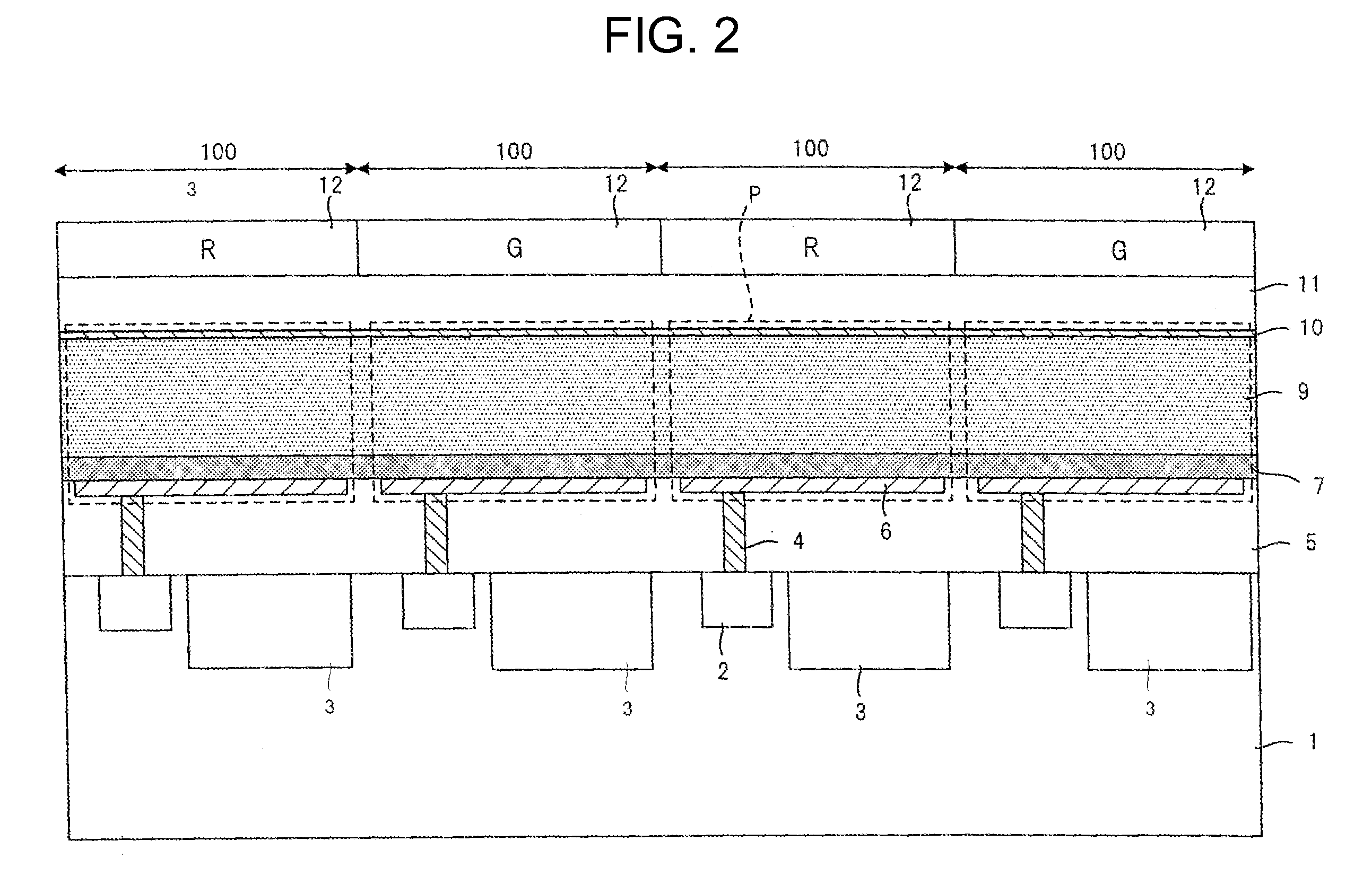
[0182]An imaging device equipped with an organic photoelectric conversion device was fabricated. However, in the imaging device, the formation of configurations above a counter electrode was omitted. The procedures are as follows.
[0183]First of all, amorphous ITO was subjected to thin film fabrication in a thickness of 30 nm on a CMOS substrate in which read-out circuits composed of a CMOS circuit and connection electrodes to be connected thereto had been formed, by a sputtering method, followed by patterning to form a pixel electrode on each of the connection electrodes. Subsequently, Compound 2 was subjected to thin film fabrication in a thickness of 100 nm on the plural pixel electrodes by a vacuum vapor deposition method, thereby forming an electron blocking layer. Subsequently, Compound 1 as a p-type organic material and fullerene (C60) as an n-type organic material were subjected to thin film fabrication in a thickness as reduced into a single layer of 100 nm and 200 nm, respe...
example 2
[0185]An imaging device was fabricated in the same manner as in Example 1, except that Compound 1 was changed to Compound 3, and the electron spin number of the photoelectric conversion layer was identified in the same manner as in Example 1.
example 3
[0186]An imaging device was fabricated in the same manner as in Example 1, except that Compound 1 was changed to Compound 4, and the electron spin number of the photoelectric conversion layer was identified in the same manner as in Example 1.
PUM
 Abstract
Description
Claims
Application Information
 - R&D
- Intellectual Property
- Life Sciences
- Materials
- Tech Scout
- Unparalleled Data Quality
- Higher Quality Content
- 60% Fewer Hallucinations
Browse by: Latest US Patents, China's latest patents, Technical Efficacy Thesaurus, Application Domain, Technology Topic, Popular Technical Reports.
© 2025 PatSnap. All rights reserved.Legal|Privacy policy|Modern Slavery Act Transparency Statement|Sitemap|About US| Contact US: help@patsnap.com