Display device and manufacturing method thereof

a technology of a display device and a manufacturing method, applied in the field of display devices, can solve the problems of variation in the characteristics of the transistor, inability to expect further high performance, and slow operation speed of the thin film transistor using amorphous silicon, etc., and achieve the effect of increasing the operation speed of the transistor, holding stably, and displaying stably

Active Publication Date: 2011-07-28
SEMICON ENERGY LAB CO LTD
View PDF101 Cites 21 Cited by
  • Summary
  • Abstract
  • Description
  • Claims
  • Application Information

AI Technical Summary

Benefits of technology

[0012]It is an object of one embodiment of the present invention to provide a display device including a transistor having stable electric characteristics (e.g., an off current is extremely reduced).
[0013]One embodiment of the present invention provides a display device having high image quality by using a transistor whose off current is reduced to an extremely low level. In order to reduce off current of a transistor, a semiconductor material whose width of a forbidden band (a band gap) is greater than that of a silicon semiconductor is used for forming a transistor, and the concentration of an impurity which serves as a carrier donor of the semiconductor material is reduced, in one embodiment of the present invention. Therefore, an oxide semiconductor whose energy gap is greater than or equal to 2 eV, preferably greater than or equal to 2.5 eV, more preferably greater than or equal to 3 eV is used for a semiconductor layer of a transistor (a layer forming a channel formation region) to reduce the concentration of an impurity which serves as a carrier donor in the oxide semiconductor. Consequently, the off current of the transistor per micrometer in channel width can be reduced to lower than 10 zA / μm at room temperature and lower than 100 zA / μm at 85° C., which is an extremely low level.
[0015]Note that a source electrode and a drain electrode of the transistor may contain a metal nitride. A gate electrode of the transistor may be provided on a lower side (a substrate side), an upper side (the side opposite to the substrate side), or both sides of the oxide semiconductor layer with an insulating layer interposed therebetween. Further, the transistor whose maximum field-effect mobility is greater than or equal to 5 cm2 / Vsec, preferably 10 cm2 / Vsec to 150 cm2 / Vsec in an on state is used. This is because by increasing the operation speed of the transistor, writing operation or the like can be performed rapidly even when density of a pixel is increased.
[0016]According to one embodiment of the present invention, a signal voltage applied to a pixel can be held stably by using a transistor whose off current is satisfactorily reduced. Consequently, a signal input to the pixel can be kept in a given state (the state in which an image signal is written), so that an image can be displayed stably. By reducing voltage fluctuation of a pixel, multi-grayscale display can be easily carried out.

Problems solved by technology

Since operation speed of a thin film transistor using amorphous silicon is slow and any further high performance cannot be expected, development of a thin film transistor using polysilicon has been underway.
However, a crystallization step is required for forming polysilicon, which leads to cause variation in transistor characteristics and inhibits enlargement of a panel area.

Method used


Image

  • Display device and manufacturing method thereof
  • Display device and manufacturing method thereof
  • Display device and manufacturing method thereof

Examples


embodiment 1

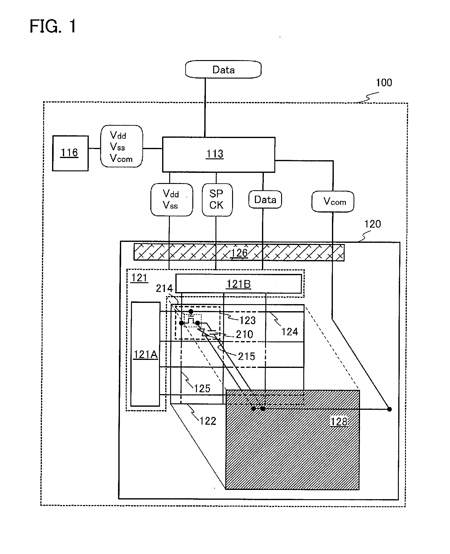
[0034]In this embodiment, one mode of a liquid crystal display device of the present invention is described with reference to FIG. 1.

[0035]An example of each component of a liquid crystal display device 100 shown in this embodiment is illustrated in a block diagram in FIG. 1. The liquid crystal display device 100 includes a power supply 116, a display control circuit 113, and a display panel 120. In the case of a transmissive liquid crystal display device or a transflective liquid crystal display device, a lighting unit (a backlight) portion may be further provided as a light source.

[0036]An image signal (an image signal Data) is supplied to the liquid crystal display device 100 from an external device which is connected to the liquid crystal display device 100. Note that power supply potential (high power supply potential Vdd, low power supply potential Vss, and common potential Vcom) is supplied by turning on the power supply 116 of the liquid crystal display device and starting s...

embodiment 2

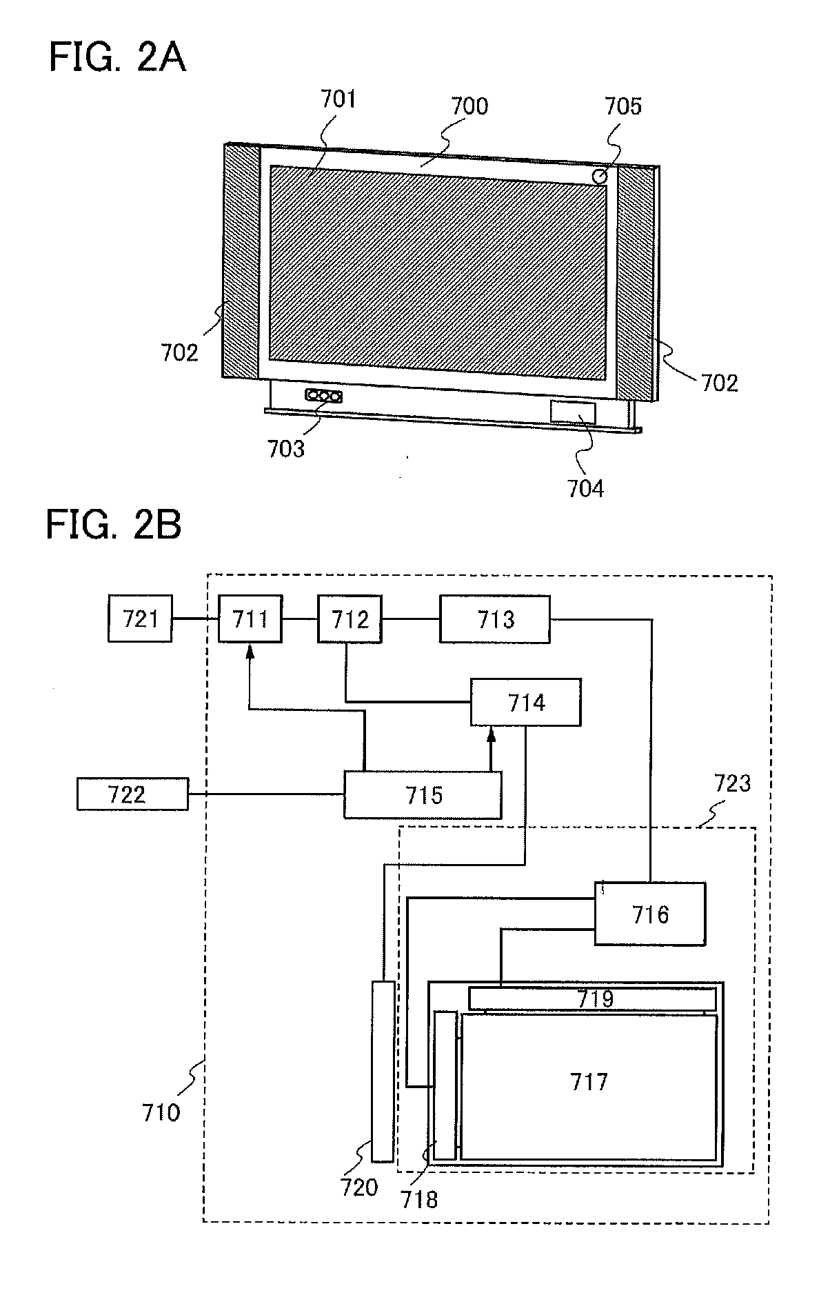
[0057]In this embodiment, an example of an electronic device including the liquid crystal display device described in Embodiment 1 will be described.

[0058]FIG. 2A illustrates an external view of a television receiver which is an electronic device. FIG. 2A illustrates a housing 700 in which a display module 701 manufactured using the display panel described in Embodiment 1 is provided. The housing 700 includes a speaker 702, operation keys 703, an external connection terminal 704, an illuminance sensor 705, and the like.

[0059]The television receiver illustrated in FIG. 2A can display text information or a still image in addition to a moving image. A moving image can be displayed in a region of a display portion while a still image can be displayed in the other region. Note that a displayed still image includes characters, diagrams, signs, pictures, designs, and paintings or a combination of any of them. Alternatively, any of the displayed images which are colored is included.

[0060]FI...

embodiment 3

[0069]In this embodiment, description is made on a structure example of a backlight (a backlight portion, a backlight unit) which can be applied to a liquid crystal display device disclosed in this specification with reference to FIGS. 4A to 4C and FIGS. 5A to 5C.

[0070]FIG. 4A illustrates an example of a liquid crystal display device including a so-called edge-light type backlight portion 5201 and a display panel 5207. An edge-light type corresponds to a type in which a light source is provided at an end of a backlight portion and light of the light source is emitted from the entire light-emitting surface.

[0071]The backlight portion 5201 includes a diffusion plate 5202 (also referred to as a diffusion sheet), a light guide plate 5203, a reflection plate 5204, a lamp reflector 5205, and a light source 5206. Note that the backlight portion 5201 may also include a luminance improvement film or the like.

[0072]The light source 5206 has a function of emitting light as necessary. For examp...


PUM

PropertyMeasurementUnit
electrostatic capacitanceaaaaaaaaaa
band gapaaaaaaaaaa
temperatureaaaaaaaaaa

Abstract

Disclosed is a display device including a transistor showing extremely low off current. In order to reduce the off current, a semiconductor material whose band gap is greater than that of a silicon semiconductor is used for forming a transistor, and the concentration of an impurity which serves as a carrier donor of the semiconductor material is reduced. Specifically, an oxide semiconductor whose band gap is greater than or equal to 2 eV, preferably greater than or equal to 2.5 eV, more preferably greater than or equal to 3 eV is used for a semiconductor layer of a transistor, and the concentration of an impurity which serves as a carrier donor included is reduced. Consequently, the off current of the transistor per micrometer in channel width can be reduced to lower than 10 zA / μm at room temperature and lower than 100 zA / μm at 85° C.

Description

TECHNICAL FIELD[0001]One embodiment of the present invention relates to a display device including a field-effect transistor using an oxide semiconductor.BACKGROUND ART[0002]A liquid crystal display panel including a thin film transistor using amorphous silicon as a driving element of liquid crystal is widely used in commercial products such as a monitor of a computer and a liquid crystal television. A manufacturing technique of a thin film transistor using amorphous silicon has been already established and a liquid crystal panel with more than 60 inches has been produced.[0003]Since operation speed of a thin film transistor using amorphous silicon is slow and any further high performance cannot be expected, development of a thin film transistor using polysilicon has been underway. However, a crystallization step is required for forming polysilicon, which leads to cause variation in transistor characteristics and inhibits enlargement of a panel area.[0004]In contrast, an oxide semic...

Claims


Application Information

Patent Timeline
Patent Type & Authority Applications(United States)
IPC IPC(8): G02F1/136
CPCG02F1/1336H01L29/12G09G3/3406G09G3/3648G09G2320/0214G09G2320/0626G09G2360/144H01L27/1225H01L27/3262H01L29/66742H01L29/78609H01L29/7869H01L29/66969G02F1/133345G02F1/136277H01L27/153G02F1/1368H10K59/1213H01L29/45G02F1/134309G09G3/3659G09G2300/08H01L29/045H01L29/24
Inventor YAMAZAKI, SHUNPEI
Owner SEMICON ENERGY LAB CO LTD
Why Eureka
Try Eureka