Method of manufacturing semiconductor device and semiconductor device
a manufacturing method and semiconductor technology, applied in the direction of film/foil adhesives without carriers, film/foil adhesives, basic electric elements, etc., can solve the problems of poor fluidity of film-type adhesives, difficult application to semiconductor devices in which semiconductor elements are located, and remains of cavities. , to achieve the effect of suppressing the occurrence of voids and excellent reliability
- Summary
- Abstract
- Description
- Claims
- Application Information
AI Technical Summary
Benefits of technology
Problems solved by technology
Method used
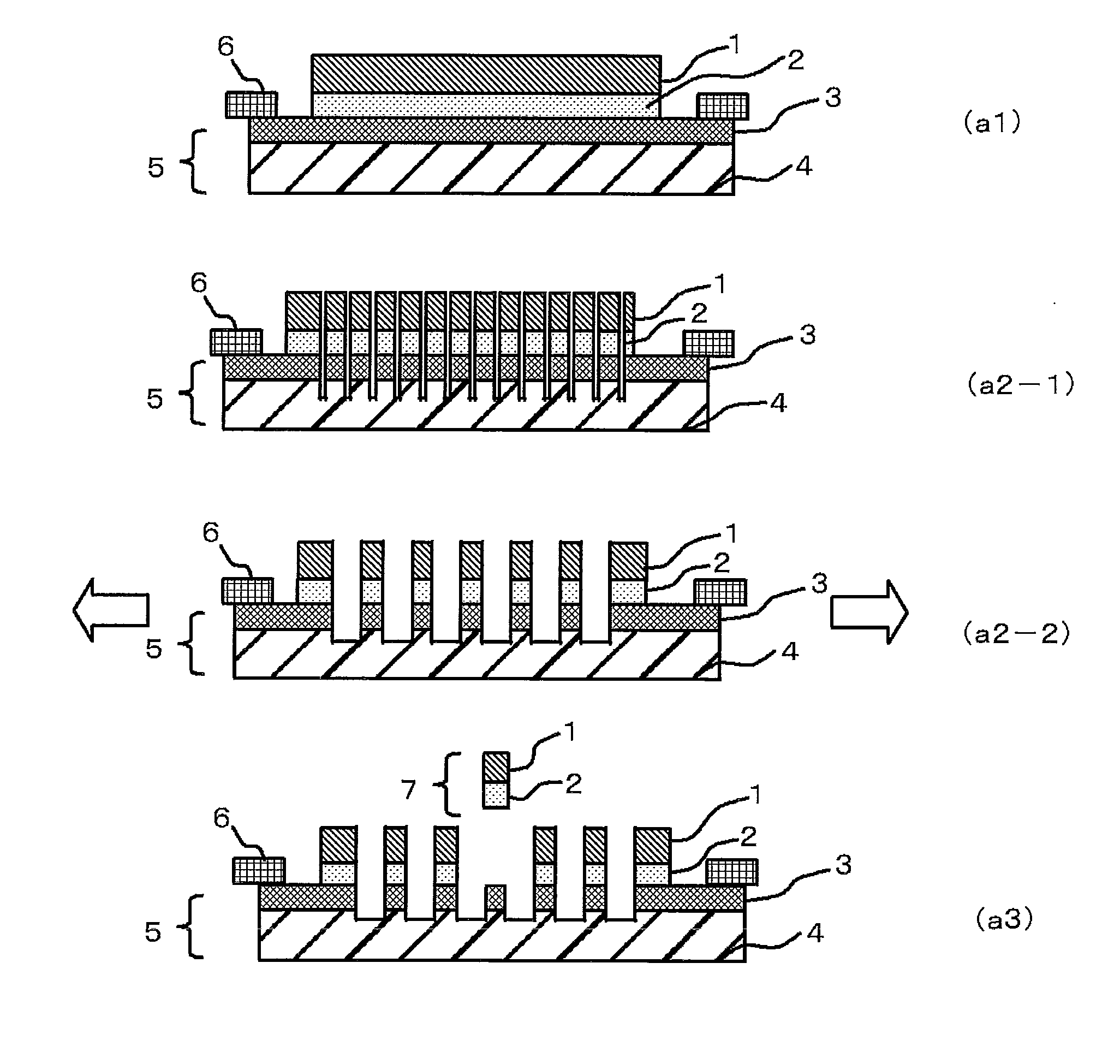
Image

Examples
example 1
Preparation of a Resin Varnish for an Adhesive Film
[0121]Following components were dissolved in methyl ethyl ketone (MEK) so as to obtain a resin wax with a resin solid content of 41%:
[0122]as the (meth)acrylic resin, 100 parts by mass of an acrylic acid ester copolymer (ethylacrylate-butylacrylate-acrylonitrile-acrylic acid-hydroxyethyl methacrylate copolymer, manufactured by Nagase ChemteX Corporation, SG-708-6, Tg: 6° C., weight-average molecular weight: 800,000);
[0123]as the epoxy resin, 105 parts by mass of EOCN-1020-80 (ortho cresol novolak-type epoxy resin, epoxy equivalent 200 g / eq, softening point 80° C., manufactured by Nippon Kayaku Co., Ltd.) and 157 parts by mass of NC3000P (aralkyl type epoxy resin, epoxy equivalent 272 g / eq, softening point 58° C., manufactured by Nippon Kayaku Co., Ltd.);
[0124]as the curing agent, 82 parts by mass of a liquid-phase phenol compound MEH-8000H (hydroxyl group equivalent 141 g / OH group, manufactured by Meiwa Plastic Industries, Ltd.) and...
PUM
| Property | Measurement | Unit |
|---|---|---|
| Temperature | aaaaa | aaaaa |
| Temperature | aaaaa | aaaaa |
| Temperature | aaaaa | aaaaa |
Abstract
Description
Claims
Application Information
 - R&D
- Intellectual Property
- Life Sciences
- Materials
- Tech Scout
- Unparalleled Data Quality
- Higher Quality Content
- 60% Fewer Hallucinations
Browse by: Latest US Patents, China's latest patents, Technical Efficacy Thesaurus, Application Domain, Technology Topic, Popular Technical Reports.
© 2025 PatSnap. All rights reserved.Legal|Privacy policy|Modern Slavery Act Transparency Statement|Sitemap|About US| Contact US: help@patsnap.com