Amplifier Circuit

a technology of amplifier circuit and amplifier, applied in the field of radio frequency (rf) circuit, can solve problems such as degradation of efficiency, and achieve the effect of reducing the effect of “friendly” signals and reducing the maintenance of signals

Inactive Publication Date: 2011-06-16
AURIGA MEASUREMENT SYST
View PDF19 Cites 12 Cited by
  • Summary
  • Abstract
  • Description
  • Claims
  • Application Information

AI Technical Summary

Benefits of technology

[0023]In one embodiment, the circuit is designed to reduce effects of “friendly” signals (e.g. on a ship with multiple radars operating at multiple frequencies and power levels, this bypass mode can be used to reduce maintain the signal (e.g. a signal processor) in a desired range.
[0024]Switching elements may be provided as any type of electronic switch, for example, from one or more of (or a combination of) one or more diodes, one or more transistors (including one or more field effect transistors) or other two or three terminal devices. Switching elements may also be provided a mechanical switch. In one embodiment, switch characteristics are selected such that no significant signal degradation occurs in the RF signal path.

Problems solved by technology

However, the amplifier input impedance can be as non-linear as the output impedance and a signal waveform can be easily distorted at the input, degrading the efficiency.

Method used


Image

  • Amplifier Circuit
  • Amplifier Circuit
  • Amplifier Circuit

Examples


Embodiment Construction

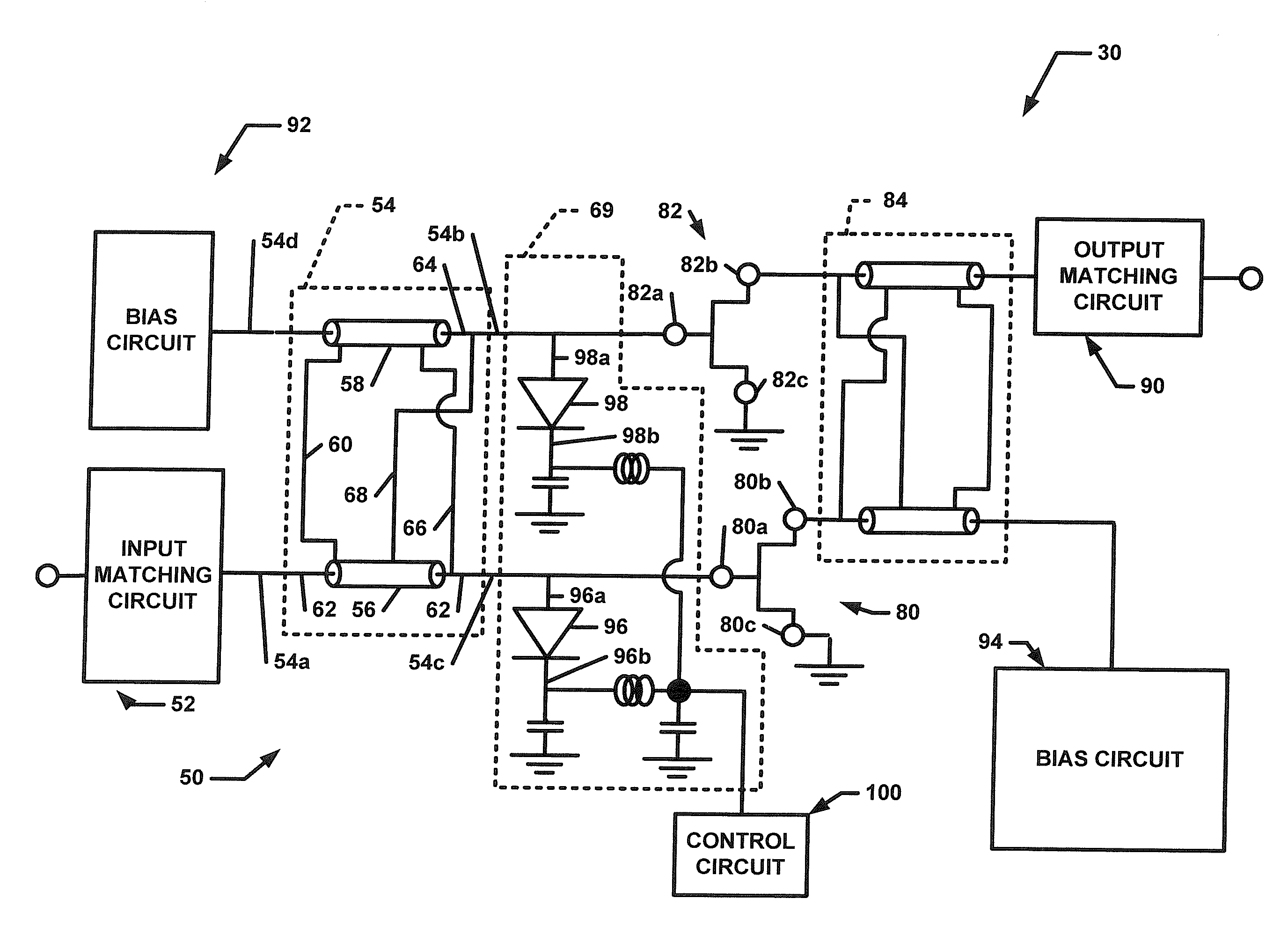
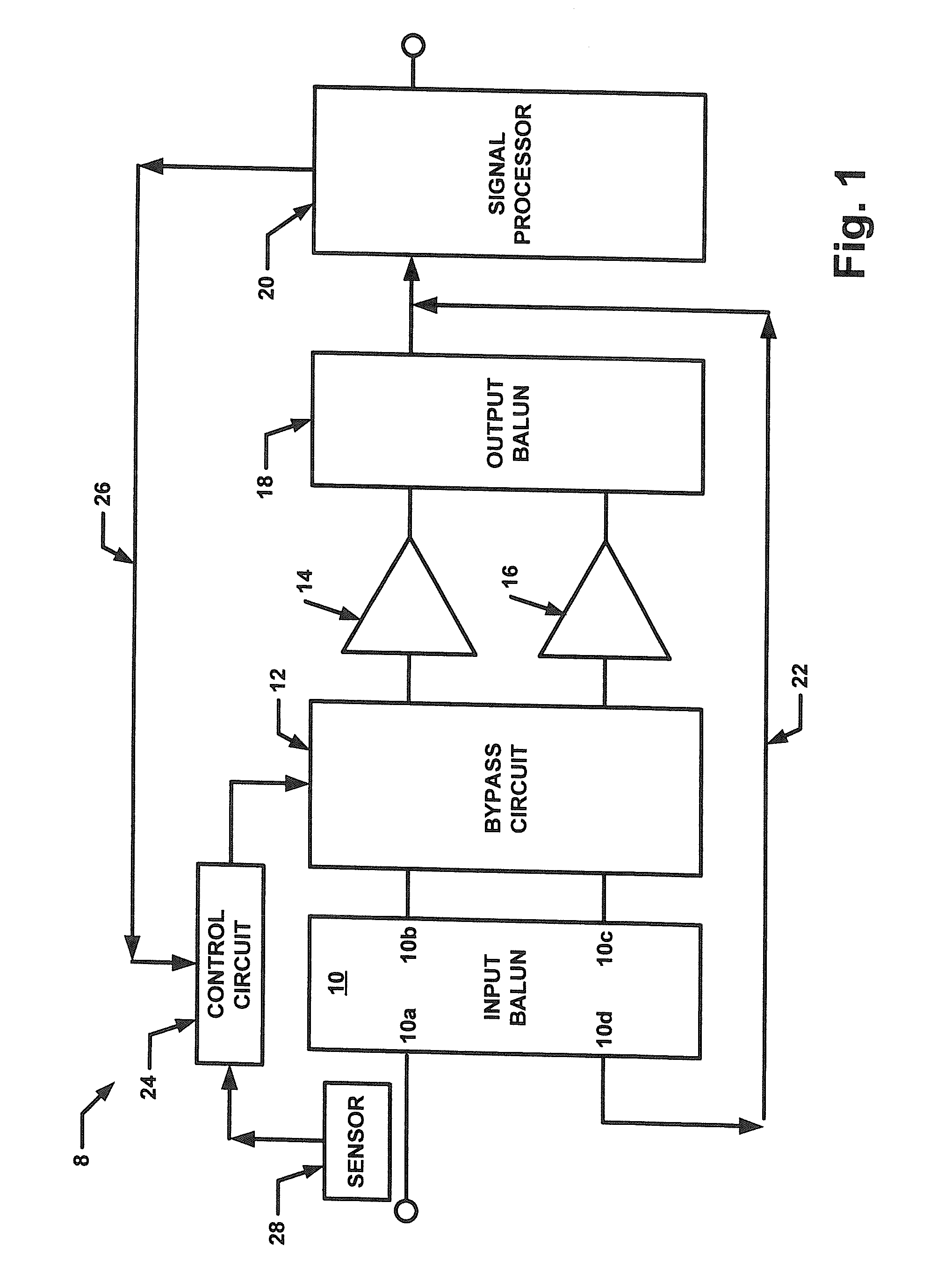
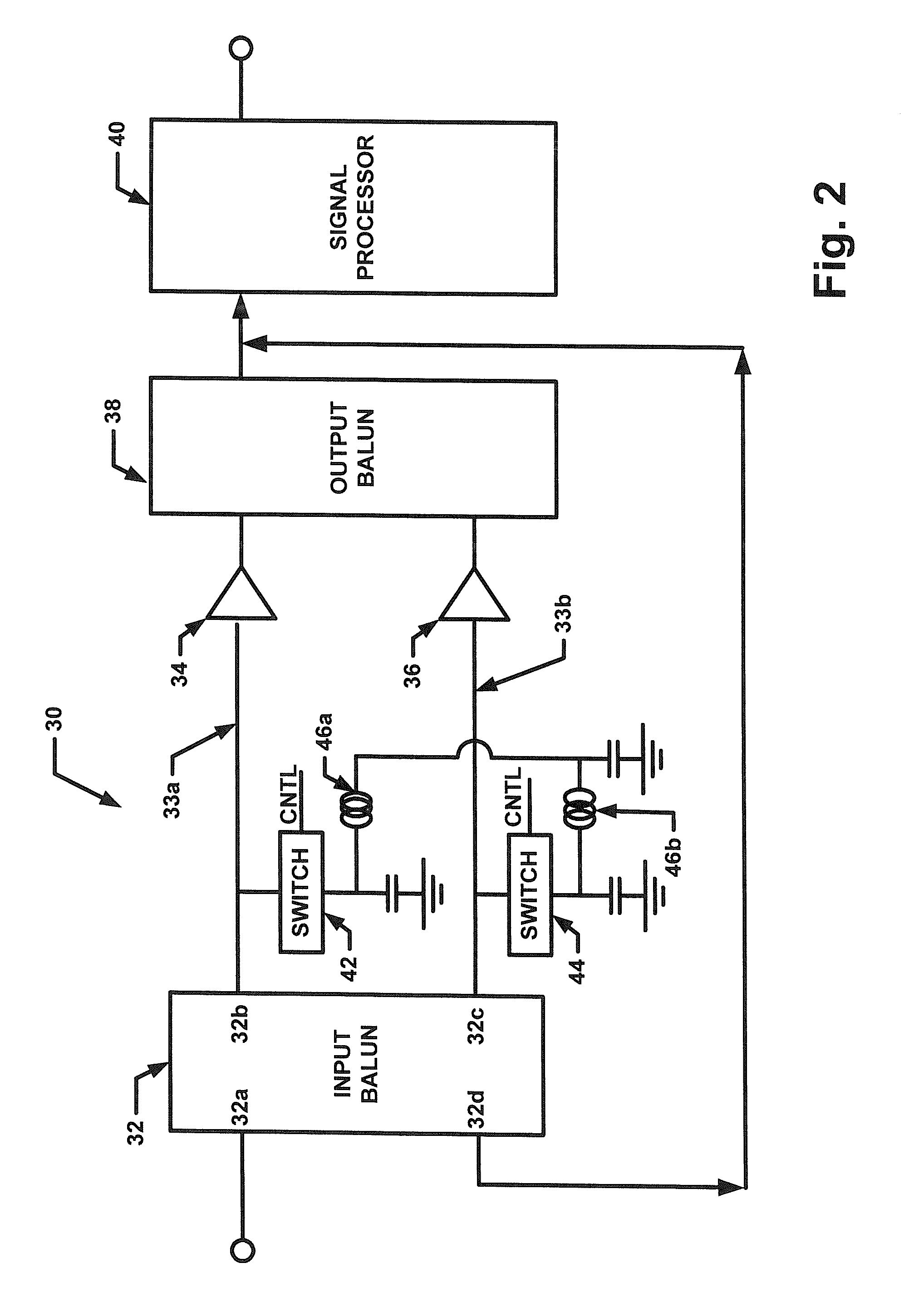
[0053]Referring now to FIG. 1, a system 8 includes an input balun 10 having a first port 10a corresponding to a radio frequency (RF) input port second and third ports 10b, 10c and bypass port 10d. An RF signal provided to input port 10a propagates through balun 10 and appear at balun ports 10b, 10c as two equal amplitude signals which are 180 degrees out of phase. Balun ports 10b, 10c are coupled to first and second ports of a bypass circuit 12. Bypass circuit 12 operates in either an amplifying mode or a bypass mode.

[0054]With bypass circuit 12 in its amplifying mode, it provides signal paths having low insertion loss characteristics between balun ports 10b, 10c and respective input ports of amplifiers 14, 16. Bypass circuit 12 maintains the phase relationship of the two RF signals provided at input balun ports 10b, 10c. Thus, the signal paths between the output ports 10b, 10c of input balun 10 and the respective input ports of amplifiers 14, 16 are ideally phase and amplitude matc...


PUM


Abstract

An amplifier circuit includes a pair of amplifying devices, a first balun coupled between an input port of the amplifier circuit and RF input ports of the pair of amplifying devices and a second balun coupled between RF output ports of the pair of amplifying devices and an output port of the amplifier circuit wherein the first and second baluns are configured such that the amplifier circuit operates under open condition for signals at a second harmonic frequency even when the second harmonic frequency is within an operating frequency band of a fundamental frequency of the amplifier circuit. In one embodiment, the amplifier circuit includes a bypass circuit which selectively couples balun ports to ground such that in response to a first control signal, the amplifier circuit operates in an amplifying mode and in response to a second control signal, the amplifier circuit operates in a bypass mode.

Description

CROSS REFERENCE TO RELATED APPLICATION[0001]This application claims the benefit of provisional application No. 61 / 286,839 filed on Dec. 16, 2009 and provisional application No. 61 / 323,472 filed on Apr. 13, 2010 under 35 U.S.C. s. 119(e) which applications are hereby incorporated herein by reference in their entireties.FIELD OF THE INVENTION[0002]The structures and techniques described herein relate to radio frequency (RF) circuits and more particularly to RF amplifier circuits.BACKGROUND OF THE INVENTION[0003]As is known in the art, a radio frequency (RF) amplifier circuit receives an RF signal at an input thereof and provides an amplified version of the RF signal at an output thereof. Ideally, the RF input signal is provided having a single frequency (the so-called fundamental frequency) and does not include any harmonic frequently signal components. Similarly, ideally, the RF amplifier provides an amplified version of the fundamental frequency RF signal and does not generate any h...

Claims


Application Information

Patent Timeline
Patent Type & Authority Applications(United States)
IPC IPC(8): H03F3/68H03F3/16H03F1/56
CPCH03F1/32H03F1/56H03F3/191H03F3/72H03F3/26H03F3/602H03F3/217
Inventor TAJIMA, YUSUKEMUIR, JOHN
Owner AURIGA MEASUREMENT SYST
Why Eureka
Try Eureka