
Architecture for operating resonant clock network in conventional mode

a clock network and conventional mode technology, applied in the direction of logic circuit coupling/interface arrangement, generating/distributing signals, pulse techniques, etc., can solve the problems of low jitter, skew, energy consumption, when designed with adequate inductance, and networks typically achieve their highest energy efficiency. , the effect of significant energy efficiency degradation

Active Publication Date: 2011-04-14
CYCLOS SEMICON
View PDF98 Cites 44 Cited by
  • Summary
  • Abstract
  • Description
  • Claims
  • Application Information

AI Technical Summary

Benefits of technology

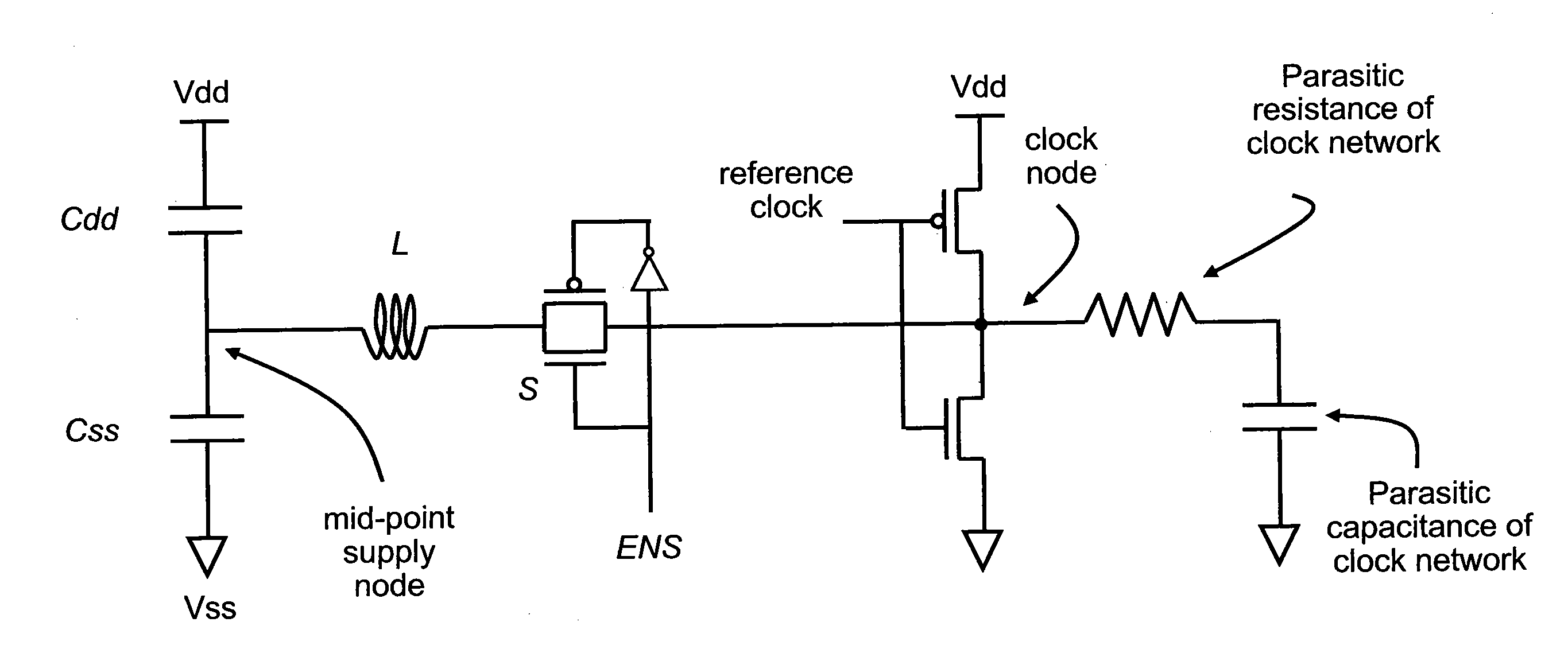
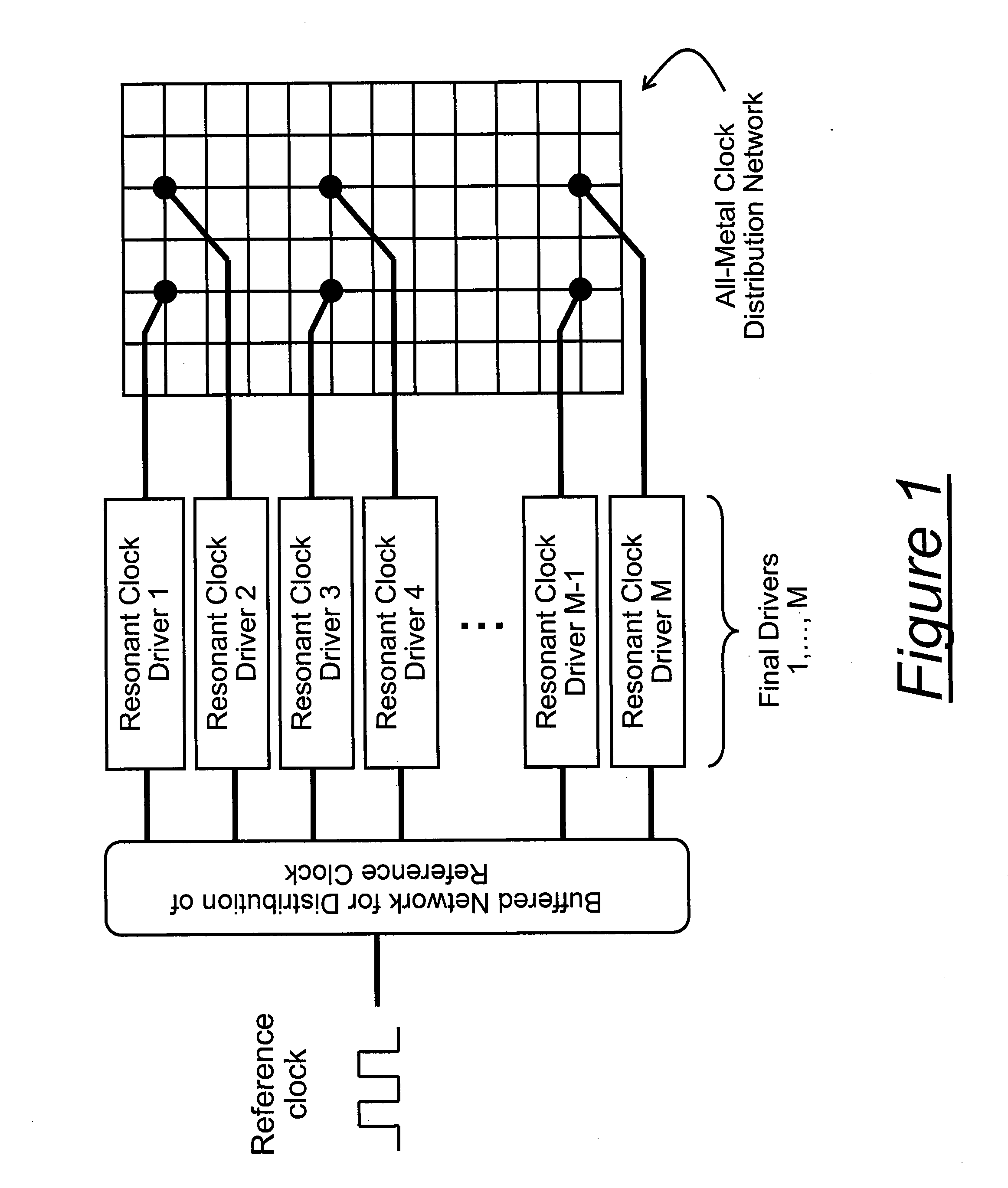
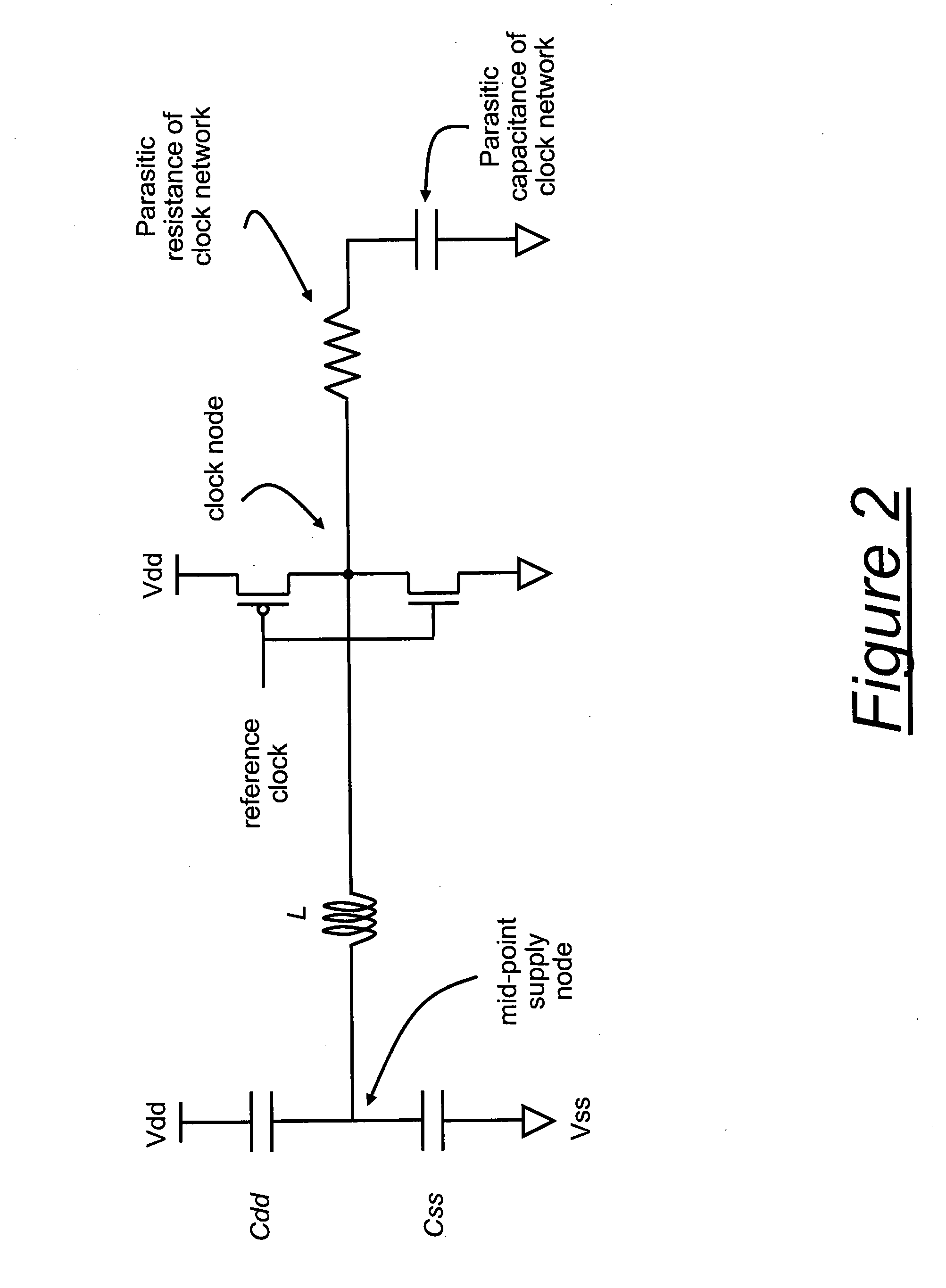
"The patent proposes an architecture for resonant clock distribution networks that allows for energy-efficient operation and meets target specifications for clock waveform. It is applicable to semiconductor devices with multiple clock frequencies, high-performance and low-power clocking requirements such as microprocessors, ASICs, and SOCs. It is also useful for at-speed testing and binning of semiconductor devices based on achievable performance levels. The patent describes a clock driver that can selectively operate either in a resonant mode or a non-resonant mode based on the state of two switch elements. The technical effects of this architecture include improved clock waveform quality, reduced power consumption, and improved performance of semiconductor devices."

Problems solved by technology

Overall network performance depends on operating speed and total network inductance, resistance, size, and topology, with lower-resistance symmetric networks resulting in lower jitter, skew, and energy consumption when designed with adequate inductance.
The challenge with the deployment of resonant clock distribution networks in multi-frequency operation contexts is that these networks typically achieve their highest energy efficiency for a relatively narrow range of clock frequencies centered around the natural frequency of the resonant network.
For clock frequencies outside this narrow range, energy efficiency degrades significantly, and to an extent that outweighs the inherent energy advantages of resonant clocking.
For example, consider a microprocessor that has been designed with a target frequency of 3 GHz, but its digital logic can only achieve a peak clock rate of 2 GHz after manufacturing.
In a resonant clock design, however, if the resonant clock network operates at 2 GHz, instead of its natural frequency of 3 GHz, its power consumption may significantly exceed the power consumption of the non-resonant design at 2 GHz.
In addition to excessive power consumption, when a resonant clock network operates away from its natural frequency, the shape of the clock waveform is increasingly deformed, as the mismatch between the natural and the operating frequency increases.
In extreme situations, the peak clock frequency after manufacturing may be so far from the natural frequency of the resonant clock network that the clock waveform at the peak clock frequency becomes deformed to such an extent that incorrect operation of the clocked elements results, and the function of the overall device becomes faulty.
At-speed testing presents yet another challenge related with the use of resonant clock distribution networks in digital devices.
Therefore, switching from scan-in mode to at-speed-test mode (or from at-speed-test mode to scan-out mode) is a challenge, due to the requirement for full-amplitude clock signals right from the beginning of the at-speed-test mode, and due to the difference in the clock frequencies between the scan modes and the at-speed-test mode.
Moreover, the resonant clock distribution networks described in these articles do not describe any approaches for disabling their inductive elements
However, the article does not provide any specifics of such a clock network design, such as circuit topologies and any design and optimization issues associated with them, and therefore is purely conceptual with respect to the use of conventional mode operation.

Method used


Image

  • Architecture for operating resonant clock network in conventional mode
  • Architecture for operating resonant clock network in conventional mode
  • Architecture for operating resonant clock network in conventional mode

Examples


Embodiment Construction

[0027]Various examples of the invention will now be described. The following description provides specific details for a thorough understanding and enabling description of these examples. One skilled in the relevant art will understand, however, that the invention may be practiced without many of these details. Likewise, one skilled in the relevant art will also understand that the invention can include many other obvious features not described in detail herein. Additionally, some well-known structures or functions may not be shown or described in detail below, so as to avoid unnecessarily obscuring the relevant description.

[0028]The terminology used below is to be interpreted in its broadest reasonable manner, even though it is being used in conjunction with a detailed description of certain specific examples of the invention. Indeed, certain terms may even be emphasized below; however, any terminology intended to be interpreted in any restricted manner will be overtly and specific...


PUM


Abstract

An architecture for resonant clock distribution networks is proposed. The proposed architecture allows for the energy-efficient operation of the resonant clock distribution network in conventional mode, so that it meets target specifications for the clock waveform. Such an architecture is generally applicable to semiconductor devices with multiple clock frequencies, and high-performance and low-power clocking requirements such as microprocessors, ASICs, and SOCs. Moreover, it is applicable to at-speed testing and to binning of semiconductor devices according to achievable performance levels.

Description

CLAIM OF PRIORITY AND RELATED APPLICATIONS[0001]This patent application is a conversion of and claims priority to U.S. Provisional Patent Application No. 61 / 250,830, entitled SYSTEMS AND METHODS FOR RESONANT CLOCKING INTEGRATED CIRCUITS, filed Oct. 12, 2009, which is incorporated herein in its entirety. This patent application is related to the technologies described in the following patents and applications, all of which are incorporated herein in their entireties:U.S. patent application Ser. No. 12 / 125,009, entitled RESONANT CLOCK AND INTERCONNECT ARCHITECTURE FOR DIGITAL DEVICES WITH MULTIPLE CLOCK NETWORKS, filed Oct. 12, 2009, which claims priority to U.S. Provisional Patent Application No. 60 / 931,582, entitled RESONANT CLOCK AND INTERCONNECT ARCHITECTURE FOR PROGRAMMABLE LOGIC DEVICES, filed May 23, 2007;U.S. patent application Ser. No. ______, entitled RESONANT CLOCK DISTRIBUTION NETWORK ARCHITECTURE WITH PROGRAMMABLE DRIVERS, filed concurrently herewith;U.S. patent applicati...

Claims


Application Information

Patent Timeline
Patent Type & Authority Applications(United States)
IPC IPC(8): H03B5/12
CPCG06F1/10H03K5/05G06F1/04H03K3/012H03K5/00H03K5/1565G06F1/06
Inventor PAPAEFTHYMIOU, MARIOS C.ISHII, ALEXANDER
Owner CYCLOS SEMICON
Learn More