
Semiconductor device and manufacturing method therefor

a semiconductor device and manufacturing method technology, applied in the field of semiconductor devices and manufacturing technologies, can solve the problem that wire bonding cannot be carried out, and achieve the effects of enhancing the reliability reducing the size and thickness of the semiconductor device, and suppressing the production of a solder bridg

Active Publication Date: 2011-03-31
RENESAS ELECTRONICS CORP
View PDF4 Cites 22 Cited by
  • Summary
  • Abstract
  • Description
  • Claims
  • Application Information

AI Technical Summary

Benefits of technology

[0011]To reduce the size of a semiconductor device with a wire bonding coupling structure, the following processing is carried out as illustrated in the comparative example in FIG. 60: the outer dimensions of a die pad 53 for placing a semiconductor chip 52 are made smaller than the outer dimensions of the semiconductor chip 52; and one end of each of multiple leads (lead terminals) 54 arranged around the die pad 53 is brought close to the semiconductor chip 52 (or the die pad 53) as much as possible. This shortens the distance from each lead 54 to a corresponding chip end (edge) of the semiconductor chip 52; therefore, the length of each side of the semiconductor device 51 is reduced and the semiconductor device 51 can be reduced in size.
[0016]The invention has been made in consideration of the above problems and it is an object thereof to provide a technology with which the size and thickness of a semiconductor device can be reduced.
[0023]It is possible to suppress production of a solder bridge during solder mounting to a mounting board or the like and to reduce the size and thickness of a semiconductor device and further enhance the reliability of the semiconductor device.

Problems solved by technology

However, when an attempt is made to reduce the size of a semiconductor device with a wire bonding coupling structure, the following problem arises:
This causes a phenomenon (problem) in which when a loop is formed, the tip of the capillary 56 and a chip end of the semiconductor chip 52 interfere with each other and wire bonding cannot be carried out.

Method used


Image

  • Semiconductor device and manufacturing method therefor
  • Semiconductor device and manufacturing method therefor
  • Semiconductor device and manufacturing method therefor

Examples


first embodiment

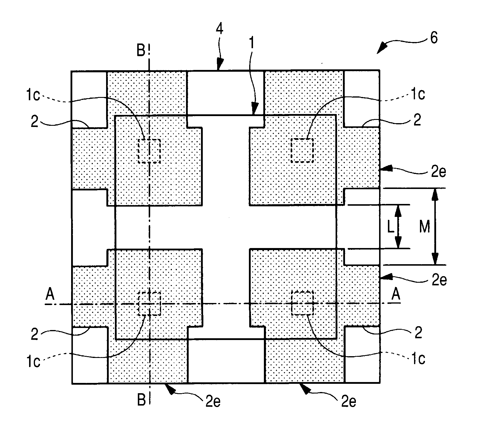
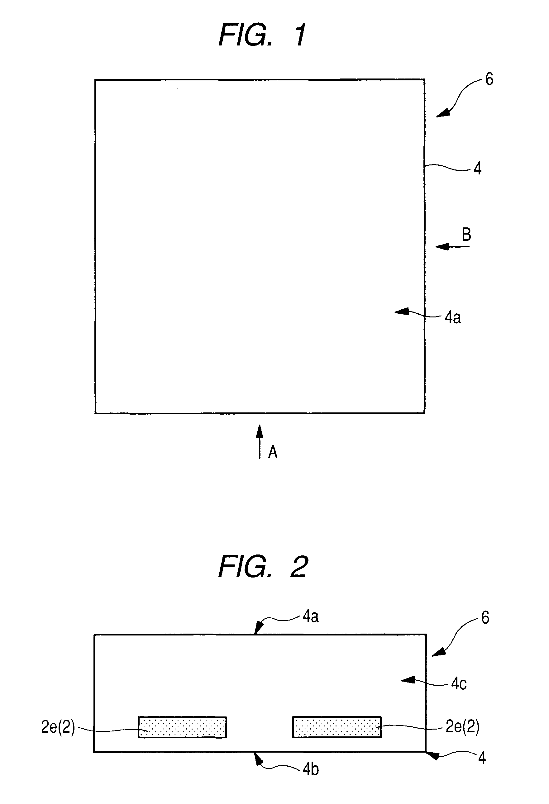
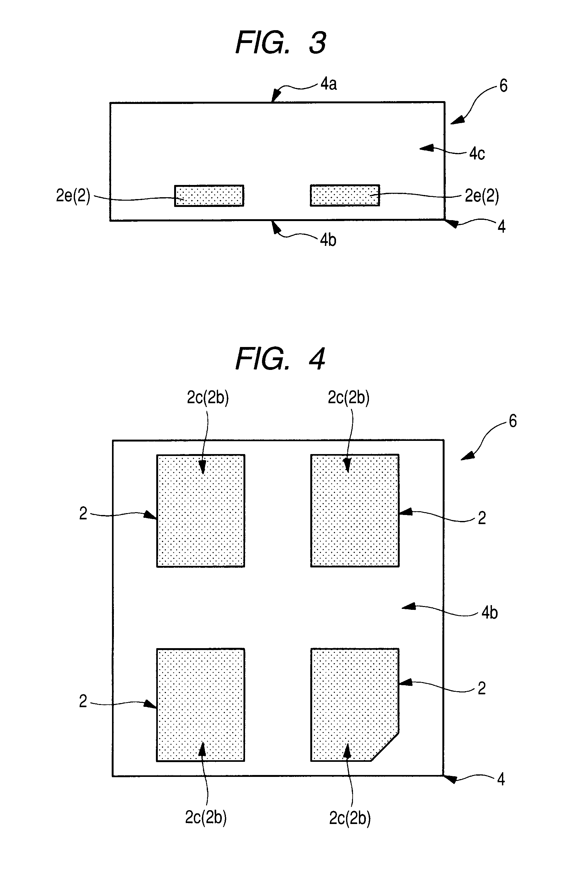
[0137]FIG. 1 is a plan view illustrating an example of the structure of a semiconductor device in the first embodiment of the invention; FIG. 2 is a side view illustrating an example of the structure of the semiconductor device illustrated in FIG. 1 as viewed from the direction A; FIG. 3 is a side view illustrating an example of the structure of the semiconductor device illustrated in FIG. 1 as viewed from the direction B; and FIG. 4 is a bottom view illustrating an example of the structure of the semiconductor device illustrated in FIG. 1 on the back surface side. FIG. 5 is a plan view illustrating an example of the structure of the semiconductor device illustrated in FIG. 1 as seen through a sealing body and a semiconductor chip; FIG. 6 is a sectional view illustrating an example of the structure cut along line A-A of FIG. 5; FIG. 7 is a sectional view illustrating an example of the structure cut along line B-B of FIG. 5; FIG. 8 is a plan view illustrating an example of half etchi...

second embodiment

[0167]FIG. 12 is a plan view illustrating an example of the structure of a semiconductor device in the second embodiment of the invention; FIG. 13 is a side view illustrating an example of the structure of the semiconductor device illustrated in FIG. 12 as viewed from the direction A; FIG. 14 is a side view illustrating an example of the structure of the semiconductor device illustrated in FIG. 12 as viewed from the direction B; FIG. 15 is a bottom view illustrating an example of the structure of the semiconductor device illustrated in FIG. 12 on the back surface side; and FIG. 16 is a plan view illustrating an example of the structure of the semiconductor device illustrated in FIG. 12 as seen through a sealing body and a semiconductor chip. FIG. 17 is a sectional view illustrating an example of the structure cut along line A-A of FIG. 16; FIG. 18 is a sectional view illustrating an example of the structure cut along line B-B of FIG. 16; FIG. 19 is a plan view illustrating an exampl...

third embodiment

[0186]FIG. 22 is a manufacturing flowchart illustrating an example of the assembling procedure for a semiconductor device in the third embodiment of the invention; FIG. 23 is a plan view illustrating an example of the structure after stud bump bonding in the assembly of the semiconductor device in FIG. 22; FIG. 24 is a plan view illustrating an example of the structure after wafer dicing in the assembly of the semiconductor device in FIG. 22; and FIG. 25 is a plan view illustrating an example of the structure after frame tape sticking in the assembly of the semiconductor device in FIG. 22. FIG. 26 is a sectional view illustrating an example of the structure cut along line A-A of FIG. 25; FIG. 27 is a plan view illustrating an example of the structure after flip chip bonding in the assembly of the semiconductor device in FIG. 22; FIG. 28 is a sectional view illustrating an example of the structure cut along line A-A of FIG. 27; FIG. 29 is a plan view illustrating an example of the st...


PUM


Abstract

The size and thickness of a semiconductor device are reduced. A semiconductor package with a flip chip bonding structure includes: a semiconductor chip having a main surface with multiple electrode pads formed therein and a back surface located on the opposite side thereto; four lead terminals each having an upper surface with the semiconductor chip placed thereover and a lower surface located on the opposite side thereto; and a sealing body having a main surface and a back surface located on the opposite side thereto. In this semiconductor package, the distance between adjacent first lower surfaces of the four lead terminals exposed in the back surface of the sealing body is made longer than the distance between adjacent upper surfaces thereof. This makes it possible to suppress the production of a solder bridge when the semiconductor package is solder mounted to a mounting board and to reduce the size and thickness of the semiconductor package and further enhance the reliability of the semiconductor package.

Description

CROSS-REFERENCE TO RELATED APPLICATIONS[0001]The disclosure of Japanese Patent Application No. 2010-72233 filed on Mar. 26, 2010 and No. 2009-223948 filed on Sep. 29, 2009 including the specification, drawings and abstract is incorporated herein by reference in its entirety.BACKGROUND OF THE INVENTION[0002]The present invention relates to semiconductor devices and manufacturing technologies therefor and in particular to a technology effectively applicable to reduction in the size and thickness of a semiconductor device.[0003]Patent Document 1 (Japanese Unexamined Patent Publication No. Hei 11 (1999)-251504) discloses a structure in which an electrode in an electronic component main body is bonded to an electrode member comprised of a lead frame by thermocompression or soldering.[0004]Patent Document 2 (Japanese Unexamined Patent Publication No. Hei 3 (1991)-94460) discloses the following structure and a manufacturing method therefor: a structure in which a semiconductor chip is flip...

Claims


Application Information

Patent Timeline
Patent Type & Authority Applications(United States)
IPC IPC(8): H01L23/498H01L21/56H01L21/60H01L23/31
CPCH01L21/4821H01L21/561H01L21/565H01L21/568H01L21/6835H01L23/3107H01L23/4951H01L23/49548H01L23/49582H01L24/11H01L24/13H01L24/16H01L24/45H01L24/81H01L24/97H01L2224/1134H01L2224/13099H01L2224/13144H01L2224/16245H01L2224/32245H01L2224/45144H01L2224/45147H01L2224/48091H01L2224/48095H01L2224/48247H01L2224/48471H01L2224/48479H01L2224/73265H01L2224/78301H01L2224/81001H01L2224/81801H01L2224/85051H01L2224/85986H01L2224/97H01L2924/01004H01L2924/01015H01L2924/01029H01L2924/01046H01L2924/01047H01L2924/0105H01L2924/01058H01L2924/01074H01L2924/01078H01L2924/01079H01L2924/01082H01L2924/14H01L2924/19041H01L2924/30105H05K3/3442H01L24/48H01L2924/01005H01L2924/01006H01L2924/01019H01L2924/01023H01L2924/01033H01L2924/014H01L2924/01028H01L24/09H01L2224/08054H01L2224/08501H01L2224/08112H01L2224/0913H01L2224/0401H01L2924/15151H01L2924/00014H01L2224/81H01L2224/85186H01L2924/00H01L2224/48227H01L23/49805H01L2224/04042H01L2924/12042H01L2924/181H01L2924/00012H01L2224/4554
Inventor NARITA, HIROAKI
Owner RENESAS ELECTRONICS CORP
Learn More