Area-Efficient Electrically Erasable Programmable Memory Cell

Active Publication Date: 2010-12-02
TEXAS INSTR INC
View PDF6 Cites 38 Cited by
  • Summary
  • Abstract
  • Description
  • Claims
  • Application Information

AI Technical Summary

Benefits of technology

[0018]Embodiments of this invention provide a memory cell structure and method of manufacturing the same that reduces the chip area
[0021]Embodiments of this invention also provide such a structure and method that eliminates cell-to-cell leakage.
[0024]According to another aspect of the invention, trench isolation structures extending to a buried oxide layer isolate the coupling capacitor from the combined sense transistor and tunneling region. This trench isolation enables the two structures to be placed closer together, further reducing the chip area required to realize the EEPROM cell. In addition, the trench isolation enables the transistor to be formed as either an n-channel or a p-channel device.

Problems solved by technology

In such embedded applications, a double-level-polysilicon process may not be available for the EEPROM if the embedding logic circuit does not require such a complex structure.
While memory cell 1 provides non-volatile data storage in a structure that can be constructed by a relatively simple process technology (i.e., single polysilicon), this construction of memory cell 1 is quite costly in terms of integrated circuit chip area.

Method used


Image

  • Area-Efficient Electrically Erasable Programmable Memory Cell
  • Area-Efficient Electrically Erasable Programmable Memory Cell
  • Area-Efficient Electrically Erasable Programmable Memory Cell

Examples


Embodiment Construction

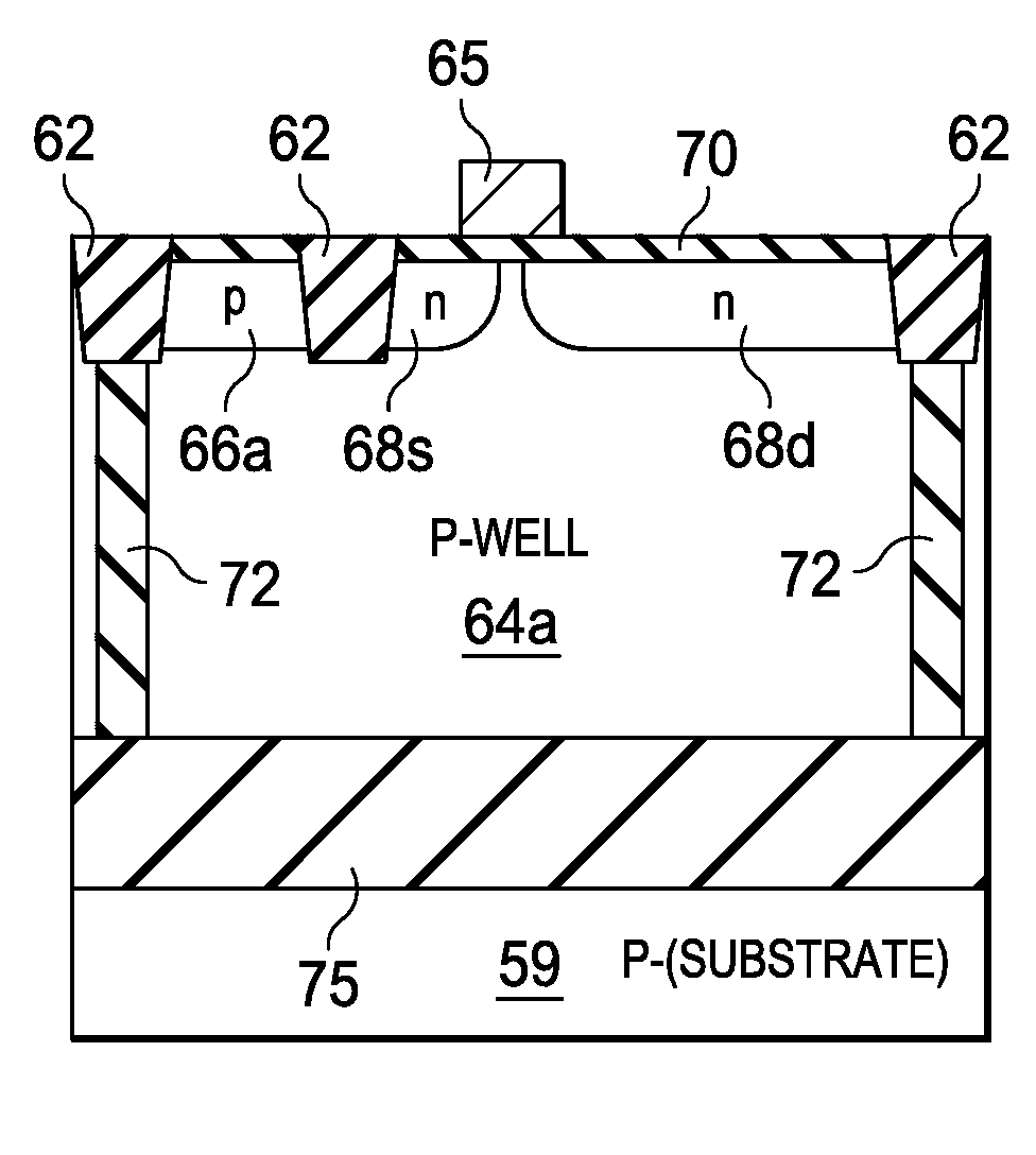
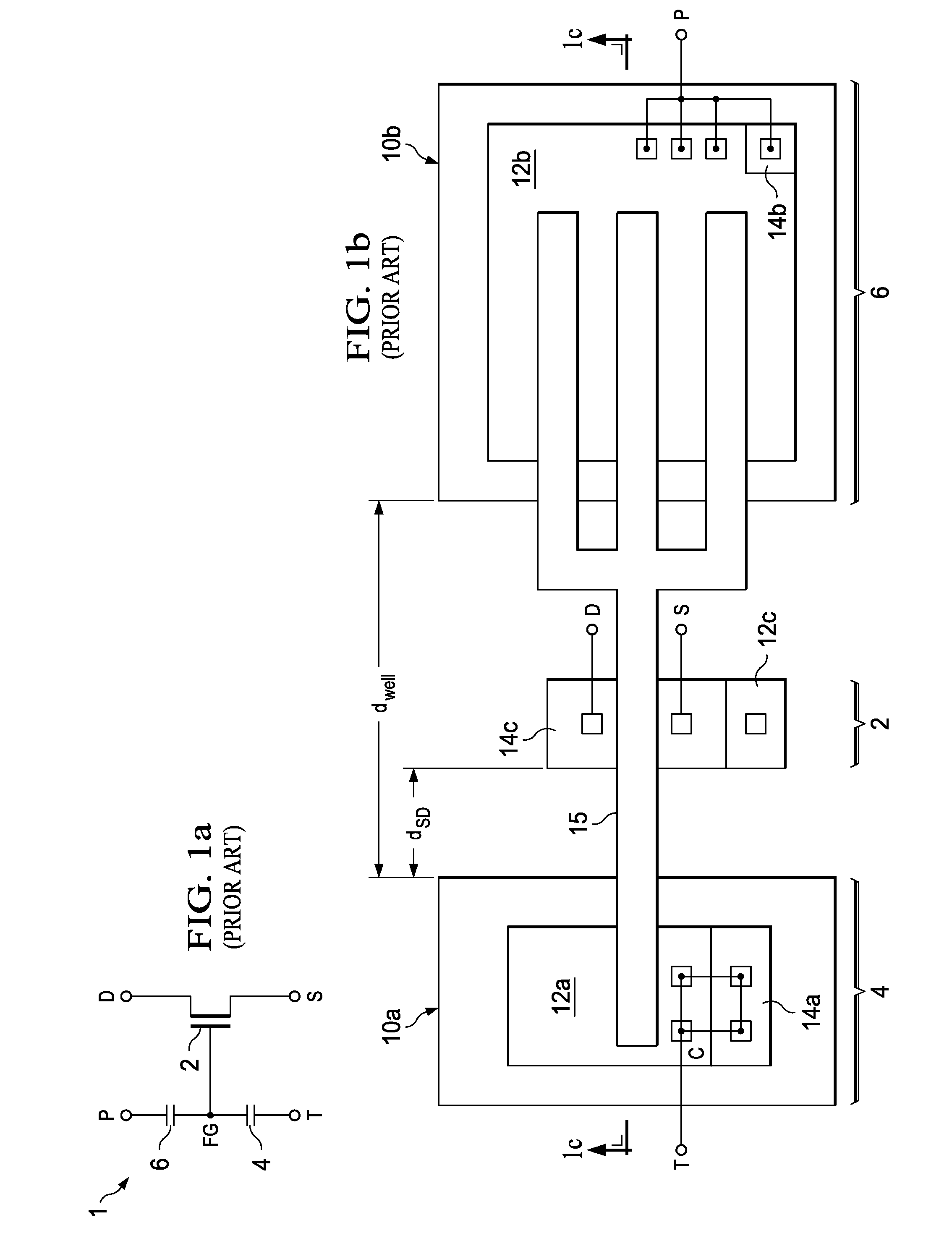
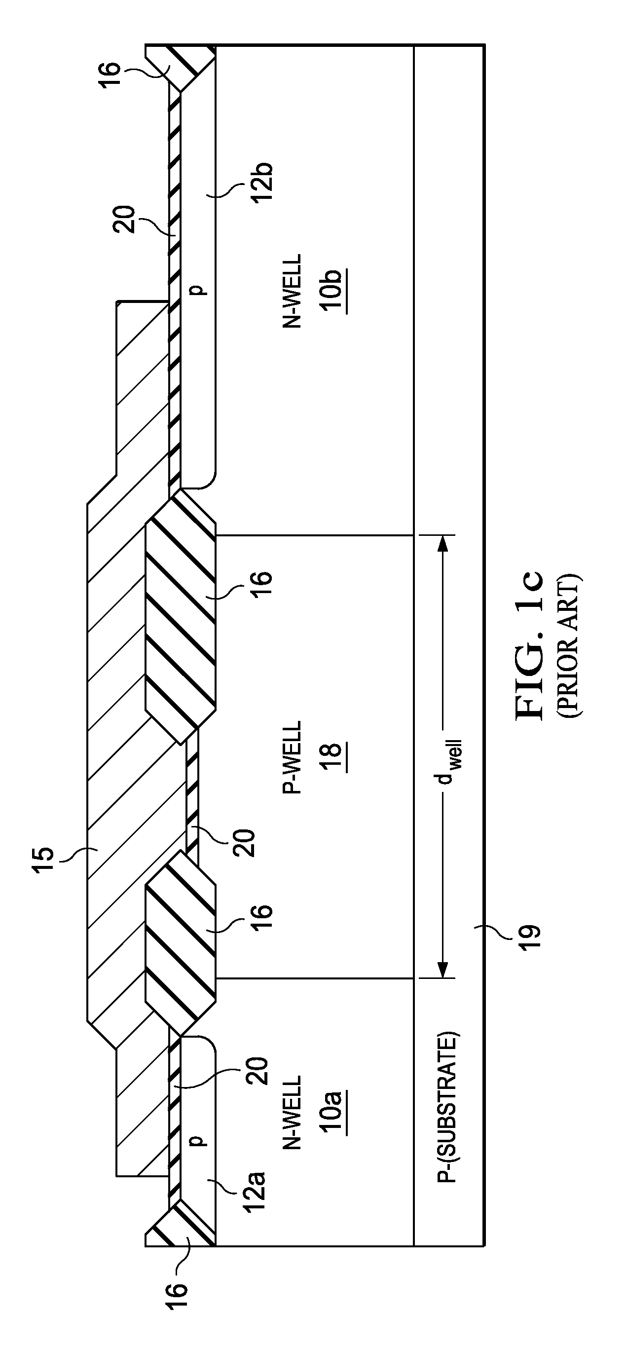
[0033]Embodiments of this invention will be described in connection with its preferred embodiment, namely as implemented into an integrated circuit including electrically erasable read-only memory functionality, particularly such functionality that is embedded into a larger scale integrated including other functional logic or other circuitry, because it is contemplated that this invention is especially beneficial when realized in such an integrated circuit. However, it is also contemplated that the benefits of this invention can be attained when implemented in other integrated circuit applications. Accordingly, it is to be understood that the following description is provided by way of example only, and is not intended to limit the true scope of this invention as claimed.

[0034]An example of an embodiment of the invention is illustrated, in functional block diagram form, in FIG. 2. Integrated circuit 35 is a large scale integrated circuit, including functional circuitry in combinatio...


PUM


Abstract

Electrically erasable programmable “read-only” memory (EEPROM) cells in an integrated circuit, and formed by a single polysilicon level. The EEPROM cell consists of a coupling capacitor and a combined read transistor and tunneling capacitor. The capacitance of the coupling capacitor is much larger than that of the tunneling capacitor. In one embodiment, field oxide isolation structures isolate the devices from one another; a lightly-doped region at the source of the read transistor improves breakdown voltage performance. In another embodiment, trench isolation structures and a buried oxide layer surround the well regions at which the coupling capacitor and combined read transistor and tunneling capacitor are formed.

Description

CROSS-REFERENCE TO RELATED APPLICATIONS[0001]Not applicable.STATEMENT REGARDING FEDERALLY SPONSORED RESEARCH OR DEVELOPMENT[0002]Not applicable.BACKGROUND OF THE INVENTION[0003]This invention is in the field of integrated circuits, and is more specifically directed to memory cell construction in electrically erasable programmable read-only memories (EEPROMs).[0004]Non-volatile solid-state read / write memory devices are now commonplace in many electronic systems, particularly in portable electronic devices and systems. A common technology for realizing non-volatile solid-state memory devices, more specifically for realizing electrically erasable programmable “read-only” memory (EEPROM) devices, utilizes “floating-gate” transistors to store the data state. According to this conventional technology, the memory cell transistor is “programmed” by biasing it so that electrons tunnel through a thin dielectric film onto an electrically isolated transistor gate element. The trapped electrons ...

Claims


Application Information

Patent Timeline
IPC IPC(8): G11C16/04H01L27/115H01L21/336G11C11/34
CPCG11C11/34G11C16/10H01L27/11519H01L27/11521H01L27/11558H01L21/76283H10B41/10H10B41/60H10B41/30
Inventor WU, XIAOJUMITROS, JOZEF CZESLAW
Owner TEXAS INSTR INC
Why Eureka
Try Eureka