
Method for growing zinc-oxide-based semiconductor device and method for manufacturing semiconductor light emitting device

a technology of zinc oxide-based semiconductors and light-emitting devices, which is applied in the direction of crystal growth process, polycrystalline material growth, natural mineral layered products, etc., can solve the problems of low productivity, high equipment cost, and use of mocvd method to directly grow zinc-oxide-based single crystals, etc., to achieve excellent flatness and crystal orientation, low defect/dislocation density, and high performance

Inactive Publication Date: 2010-11-25
STANLEY ELECTRIC CO LTD
View PDF12 Cites 12 Cited by
  • Summary
  • Abstract
  • Description
  • Claims
  • Application Information

AI Technical Summary

Benefits of technology

[0013]It is one object of the present invention to provide a method for growing on a ZnO single crystal substrate a ZnO-based single crystal which has excellent flatness and crystal orientation and a low defect / dislocation density and in which interfacial accumulation (or pileup) of impurities or diffusion of the impurities into a ZnO-based crystal growth layer is suppressed. Additionally, it is another object of the present invention to provide a semiconductor device having high performance and high reliability, especially a high-performance semiconductor light emitting device that is superior in a light-emission efficiency and a device life. Further, it is still another object of the present invention to provide a semiconductor light emitting device having a high production yield and excellent mass productivity.

Problems solved by technology

The MBE method is a crystal growth method in an ultrahigh vacuum, and it has problems that an apparatus is expensive and productivity is low.
However, utilizing the MOCVD method to directly grow a zinc-oxide-based single crystal (which will be also referred to as a ZnO-based single crystal hereinafter) on a ZnO single crystal substrate was difficult
As described above, there was a problem that a high-quality ZnO-based single crystal layer having excellent flatness and crystal orientation could not be grown on a ZnO substrate at a high temperature.
On the other hand, a manufacture problem of a ZnO substrate used for crystal growth is pointed out.
However, when growing a ZnO-based crystal on a buffer layer at a high temperature of approximately 500° C. or above, a crystal layer having poor flatness and crystal orientation is formed.

Method used


Image

  • Method for growing zinc-oxide-based semiconductor device and method for manufacturing semiconductor light emitting device
  • Method for growing zinc-oxide-based semiconductor device and method for manufacturing semiconductor light emitting device
  • Method for growing zinc-oxide-based semiconductor device and method for manufacturing semiconductor light emitting device

Examples


first embodiment

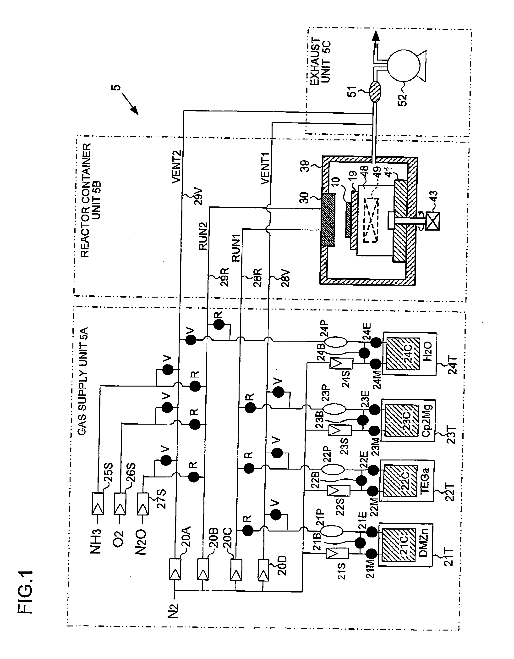
[0059]FIG. 1 schematically shows a configuration of an MOCVD apparatus 5 used for crystal growth. Particulars about an apparatus configuration of the MOCVD apparatus 5 will be described hereinafter. Further, a crystal growth material will be described later in detail.

[0060][Apparatus Configuration]

[0061]The MOCVD apparatus 5 includes a gas supply unit 5A, a reactor container unit 5B and an exhaust unit 5C. The gas supply unit 5A includes a portion that vaporizes a metalorganic (organometallic) compound material to be supplied, a portion that supplies a gaseous-material gas, and a transport unit including a function of transporting the gases.

[0062]The metalorganic compound material that is either a liquid or a solid substance at a room temperature is vaporized to be supplied. In the embodiment, DMZn (dimethyl zinc) is used as a Zinc (Zn) source, a Cp2Mg (bis-cyclopentadienyl magnesium) is used as a magnesium (Mg) source, and TEGa (triethylgallium) is used as a gallium (Ga) source, re...

second embodiment

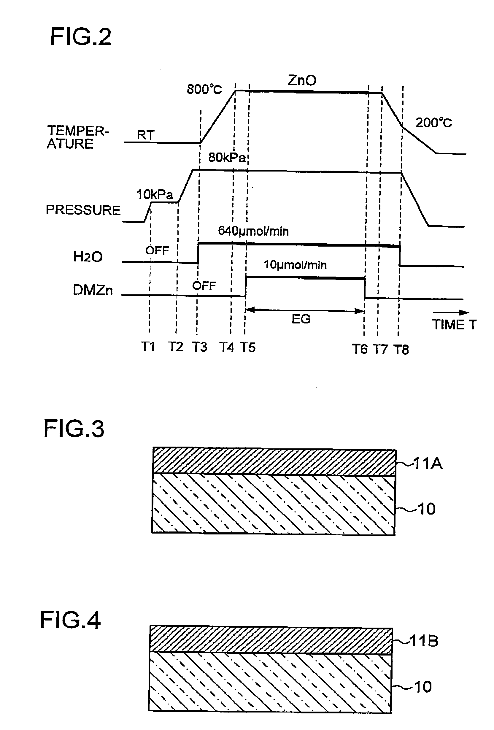
[0104]The above-described MOCVD apparatus was utilized to grow a ZnO single crystal on a ZnO single crystal substrate. In this embodiment, an ultrahigh-purity nitrogen (N2) gas whose residual O2 concentration is less than 0.1 ppm was used as a carrier gas. Moreover, a growth time (FIG. 2, EG) was set to 25 min, and an undoped ZnO single crystal layer 11B having a thickness of approximately 0.4 μm was formed as shown in FIG. 4.

[0105]It is to be noted that, besides the above-described points, a growth method including the ZnO single crystal substrate, a substrate etching treatment, a growth material, a growth sequence (FIG. 2), growth conditions and the like is the same as that in the first embodiment of the invention.

[0106]That is, in the second embodiment,[0107](1) the ZnO single crystal substrate whose FWHM of an XRD(100)ω rocking curve is less than 40 arcsec was used;[0108](2) the substrate was etched (20 min) to remove a damage layer;[0109](3) the nitrogen (N2) gas whose residual...

third embodiment

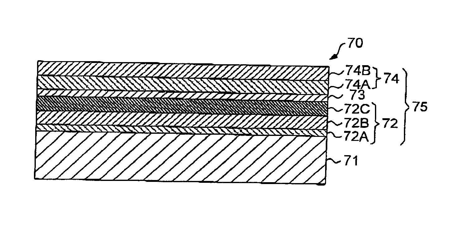
[0112]In this embodiment, the above-described MOCVD apparatus was used to grow a ZnO single crystal on a ZnO single crystal substrate and grow a ZnO-based single crystal (MgxZn(1-x)O, x=0.40) on the ZnO single crystal.

[0113]This embodiment is equal to the first and second embodiments of the invention in that a ZnO single crystal substrate whose FWHM of an XRD(100)ω rocking curve is less than 40 arcsec was used as the substrate and a surface layer was etched at a room temperature for 20 min. The growth method according to this embodiment will now be described hereinafter in detail with reference to a crystal growth sequence depicted in FIG. 5.

[0114]A ZnO single crystal substrate 10 after etching the surface layer was set on the susceptor 19, and a pressure in the reactor was adjusted to 10 kPa (a time T=T11). Additionally, the ZnO substrate 10 was rotated at 10 rpm by a rotation mechanism.

[0115]Then, a nitrogen (N2) gas was supplied to the shower head 30 from each of the first RUN li...


PUM

PropertyMeasurementUnit
temperatureaaaaaaaaaa

Abstract

A method which has a step of growing a thermostable-state ZnO-based single crystal on a ZnO single crystal substrate at a growth temperature that is equal to or greater than 600° C. and less than 900° C. by using a metalorganic compound containing no oxygen and water vapor based on an MOCVD method.

Description

BACKGROUND OF THE INVENTION[0001]1. Technical Field[0002]The present invention relates to a method for growing a zinc-oxide-based semiconductor device and a method for manufacturing a semiconductor device, and more particularly to a method for growing a zinc-oxide-based semiconductor layer on a ZnO substrate and a method for manufacturing a zinc-oxide-based semiconductor light emitting device based on an MOCVD method.[0003]2. Description of the Related Art[0004]A zinc oxide (ZnO) is a direct transition type semiconductor having band gap energy of 3.37 eV at a room temperature, and it is expected as a material for a photoelectronic device in a blue or ultraviolet region. In particular, it has physical properties very suitable for a semiconductor light emitting device, i.e., an exciton binding energy of 60 meV and a refractive index n=2.0. Further, the zinc oxide can be employed for a wide range of devices including surface-acoustic wave (SAW) devices, piezoelectric devices, and the l...

Claims


Application Information

Patent Timeline
Patent Type & Authority Applications(United States)
IPC IPC(8): H01L29/22C30B23/00B32B9/04
CPCC30B25/02H01L33/0083H01L29/22C30B29/16
Inventor HORIO, NAOCHIKAMAKISHIMA, MASAYUKI
Owner STANLEY ELECTRIC CO LTD
Learn More