Thin film transistor substrate and method of manufacturing the same
- Summary
- Abstract
- Description
- Claims
- Application Information
AI Technical Summary
Benefits of technology
Problems solved by technology
Method used
Image
Examples
embodiment 1
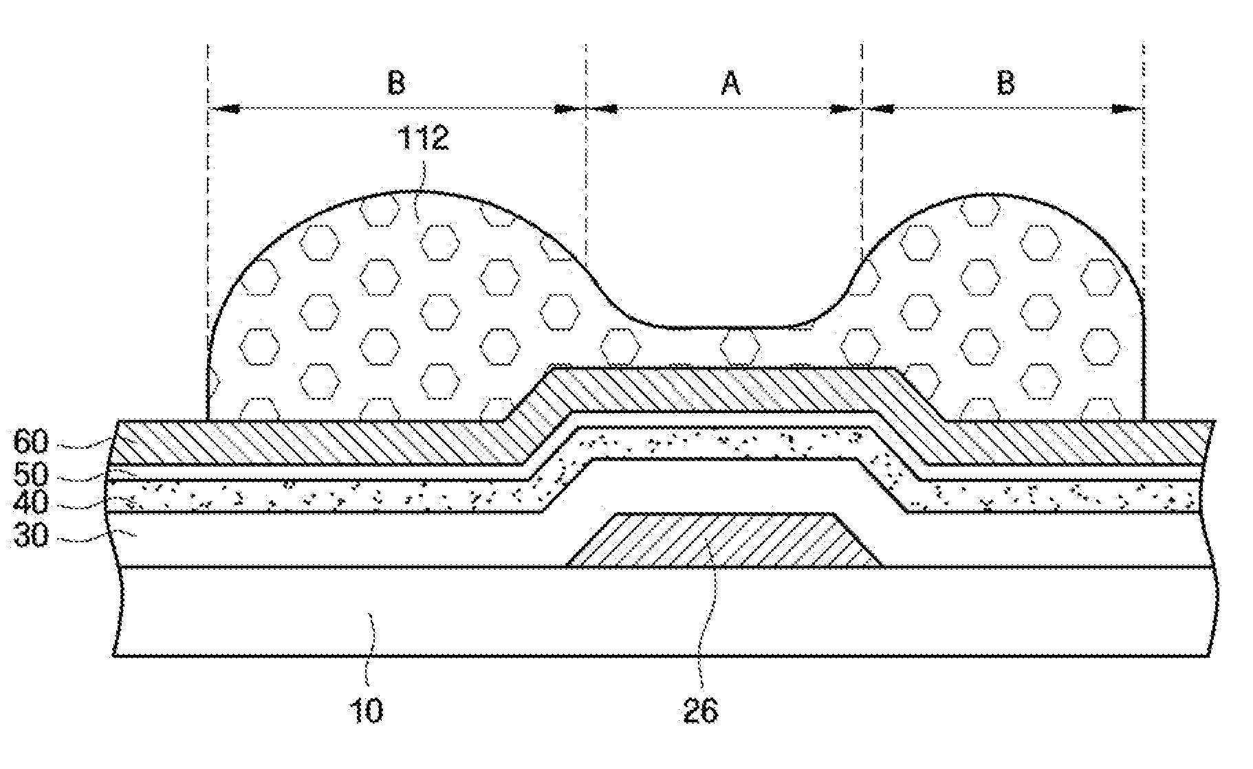
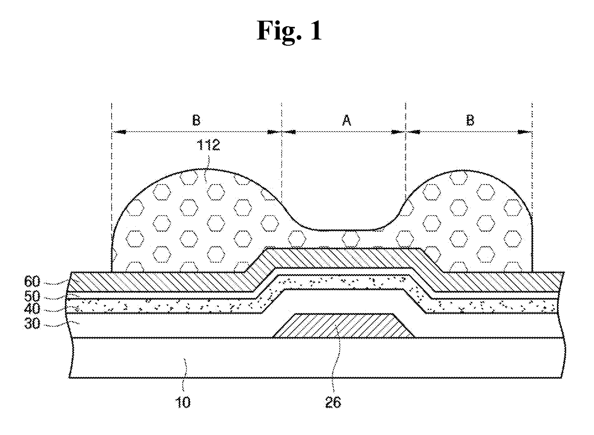
[0028]Hereinafter, an embodiment 1 of the present invention will be now described with reference to FIGS. 1-12. FIGS. 1-8 are cross-sectional views illustrating a manufacturing process of the TFT part of the TFT substrate according to the embodiment 1.
[0029]First, as shown in FIG. 1, after the gate conduction layer (not shown) is deposited on an insulating substrate 10 by a sputtering process, the gate pattern layer including a gate electrode 26 is formed by patterning the gate conduction layer through a photolithography process. Next, a gate insulating layer 30, a semiconductor layer 40, and an ohmic contact layer 50 are successively deposited on the insulating substrate 10 and on the gate pattern layer by a CVD (chemical vapor deposition) process in one example. Next, after depositing the data conduction layer 60 on the ohmic contact layer 50 by a sputtering process, for example, a photoresist pattern 112 corresponding to a data pattern layer (which will be formed from data conduc...
embodiment 2
[0044]Hereinafter, an embodiment 2 of the present invention will be now described with reference to FIGS. 1-3 and 13-17. For convenience of explanation, the components having the same function as each component illustrated in the drawings of the embodiment 1 are indicated by the same symbol and the explanation about the same structure and the same process will be omitted. The embodiment 2 will be described, focusing on the differences.
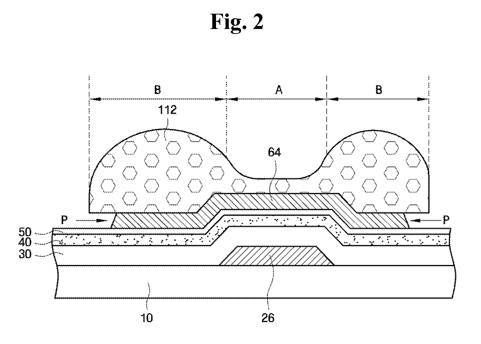
[0045]After finishing the same processes as the embodiment 1 illustrated in FIGS. 1-3 in the first instance, as shown in FIG. 13, the part of the interim data pattern layer 64 corresponding to the first region A is exposed by etch-back and ashing of the photoresist pattern 112.
[0046]Next, as shown in FIGS. 13 and 14, the data pattern layer 65, 66 including the source electrode and drain electrode is formed by etching the part of the interim data pattern layer 64 corresponding to the first region A through wet etching. In this case, the protrusion part ...
embodiment 3
[0051]Hereinafter, an embodiment 3 of the present invention will be now described with reference to FIGS. 1-3, 13-14 and 18-29. For convenience of explanation, the components having the same function as each component illustrated in the drawings of the embodiments 1 and 2 are indicated by the same symbol and the explanation about the same structure and the same process will be omitted. The embodiment 3 will be described, focusing on the differences.
[0052]After finishing the same processes as embodiment 2 illustrated in FIGS. 1-3 and 13-14 in the first instance, as shown in FIG. 18, the photoresist pattern 112 is removed.
[0053]Next, as shown in FIG. 19, a plating part 360 is formed on the two lateral surfaces and top surface of the data pattern layer 65, 66 through the electroless Ni plating method. The plating process of the present embodiment is basically the same as in the embodiments 1 and 2, but the process condition must be controlled according to the plating thickness determin...
PUM
| Property | Measurement | Unit |
|---|---|---|
| Length | aaaaa | aaaaa |
| Thickness | aaaaa | aaaaa |
| Electrical resistance | aaaaa | aaaaa |
Abstract
Description
Claims
Application Information
 - R&D
- Intellectual Property
- Life Sciences
- Materials
- Tech Scout
- Unparalleled Data Quality
- Higher Quality Content
- 60% Fewer Hallucinations
Browse by: Latest US Patents, China's latest patents, Technical Efficacy Thesaurus, Application Domain, Technology Topic, Popular Technical Reports.
© 2025 PatSnap. All rights reserved.Legal|Privacy policy|Modern Slavery Act Transparency Statement|Sitemap|About US| Contact US: help@patsnap.com


