
LDMOS with double LDD and trenched drain

a technology of ldmos and drains, which is applied in the direction of basic electric elements, electrical apparatus, and semiconductor devices, can solve the problems of large conduction loss, device damage, and high rdson between drains and sources, and achieve the effect of reducing contact resistance and reducing contact resistan

Inactive Publication Date: 2010-09-23
FORCE MOS TECH CO LTD
View PDF2 Cites 20 Cited by
  • Summary
  • Abstract
  • Description
  • Claims
  • Application Information

AI Technical Summary

Benefits of technology

[0009]It is therefore an object of the present invention to provide new and improved LDMOS cell and manufacture process to reduce the on resistance and increase breakdown voltage, while remaining a lower fabricating cost.
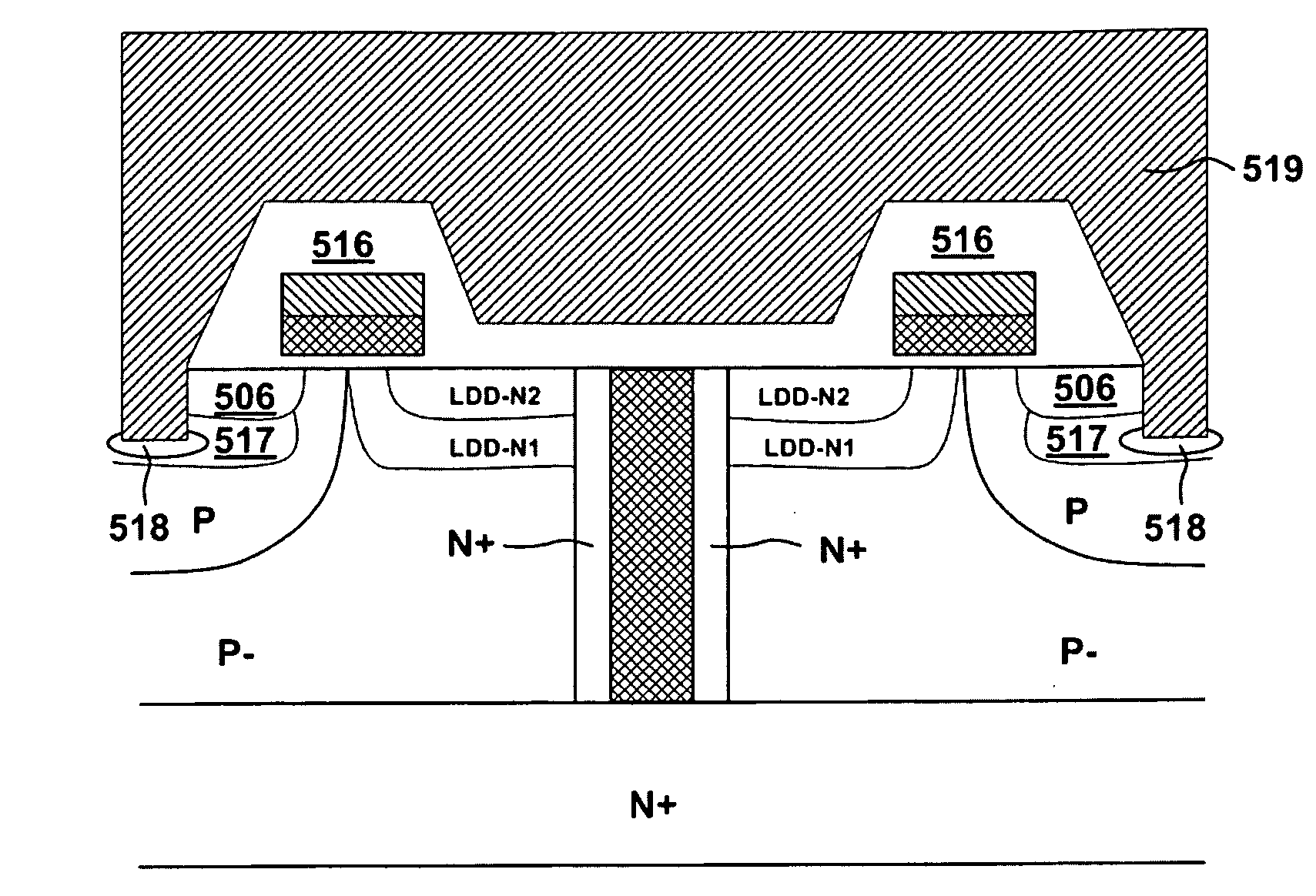
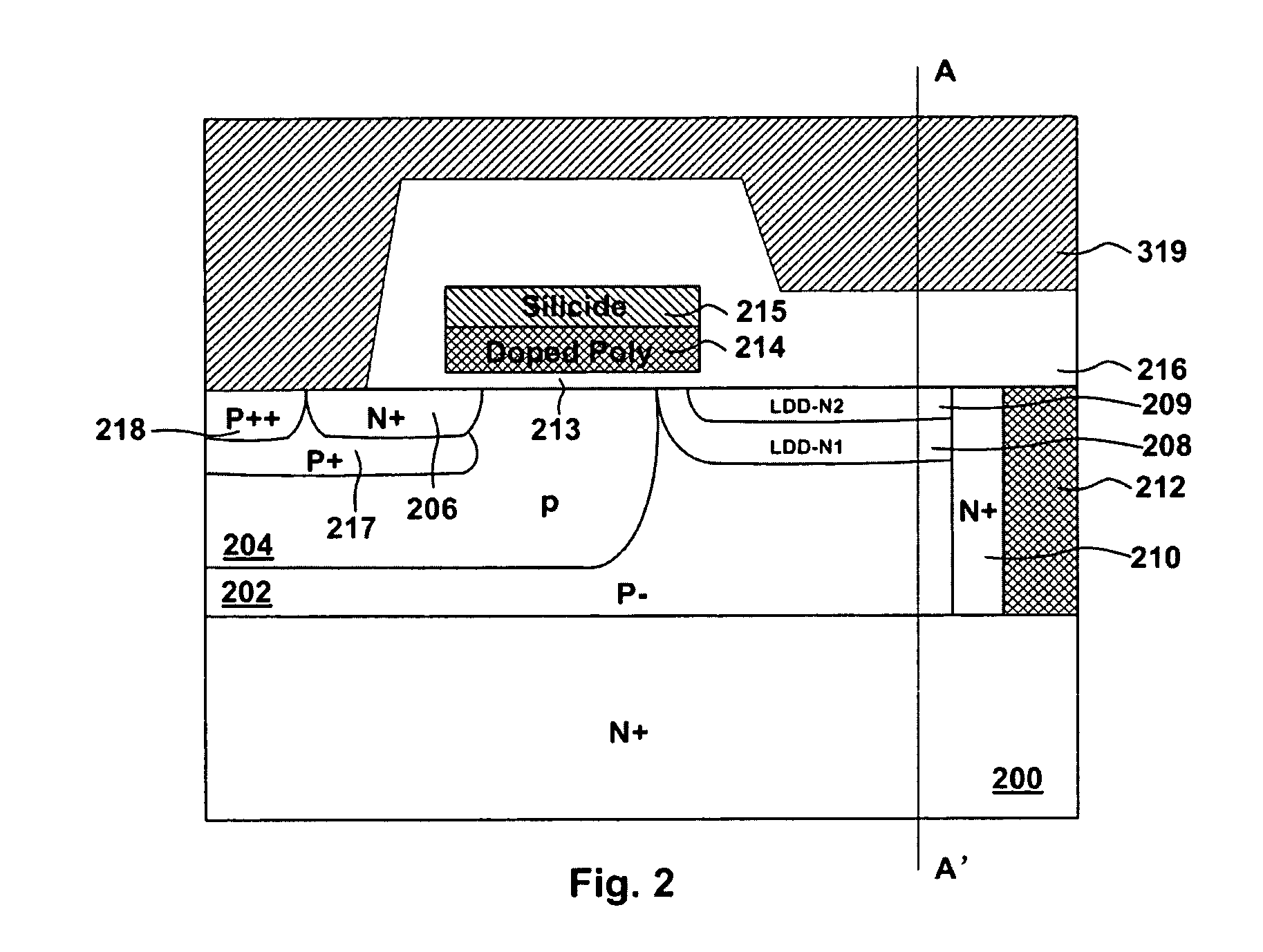
[0011]Another aspect of the present invention is that, as shown in FIG. 2, and FIGS. 3 to 8, before the source implantation, a step of P+ implantation for the formation of avalanche improved region is carried out with a concentration from 1E18 to 5E19 atoms / cm3 to form a P+ area underneath source region for reducing the base resistance in the parasitic bipolar.
[0014]Another aspect of the present invention is that, as shown in FIG. 7 and FIG. 8, the contact CD can be further shrunk with filling tungsten plug into the source-body contact trench and metal step coverage is also thus significantly improved.
[0015]Another aspect of the present invention is that, as no additional mask is required to implement the LDD-N2 implantation and P+ area during fabricating process, the device has better performance of high BV and low Rdson than the prior art without extra fabrication cost.
[0018]Briefly, in another preferred embodiment, as shown in FIG. 5, the present invention disclosed a similar LDMOS cell to structure in FIG. 2 except that, a second trench serving as source-body contact trench is etched through said second insulating layer and said source region, and into said the P+ avalanche improved region or through P+ avalanche improved region into P body region. Accordingly, said P++ body contact doping region area is formed around the bottom of said second trench to provide a low resistance contact between body region and source metal filled into said second trench.
[0020]Briefly, in another preferred embodiment, as shown in FIGS. 7 and 8, the present invention disclosed a similar LDMOS cell to structures in FIGS. 5 and 6, respectively. The devices further comprises the source-body contact trench padded with a barrier layer composed of Ti / TiN or Co / TiN and filled with tungsten contact plugs for contacting the body regions and source regions. Each of these source contact trenches further are extended into body regions having a body contact doping region implanted below the contact trenches to reduce the contact resistance. The top surface of the second insulation layer is covered with a metal resistance-reduction interlayer composed of Ti or Ti / TiN for reducing contact resistance between the tungsten plug and source metal.

Problems solved by technology

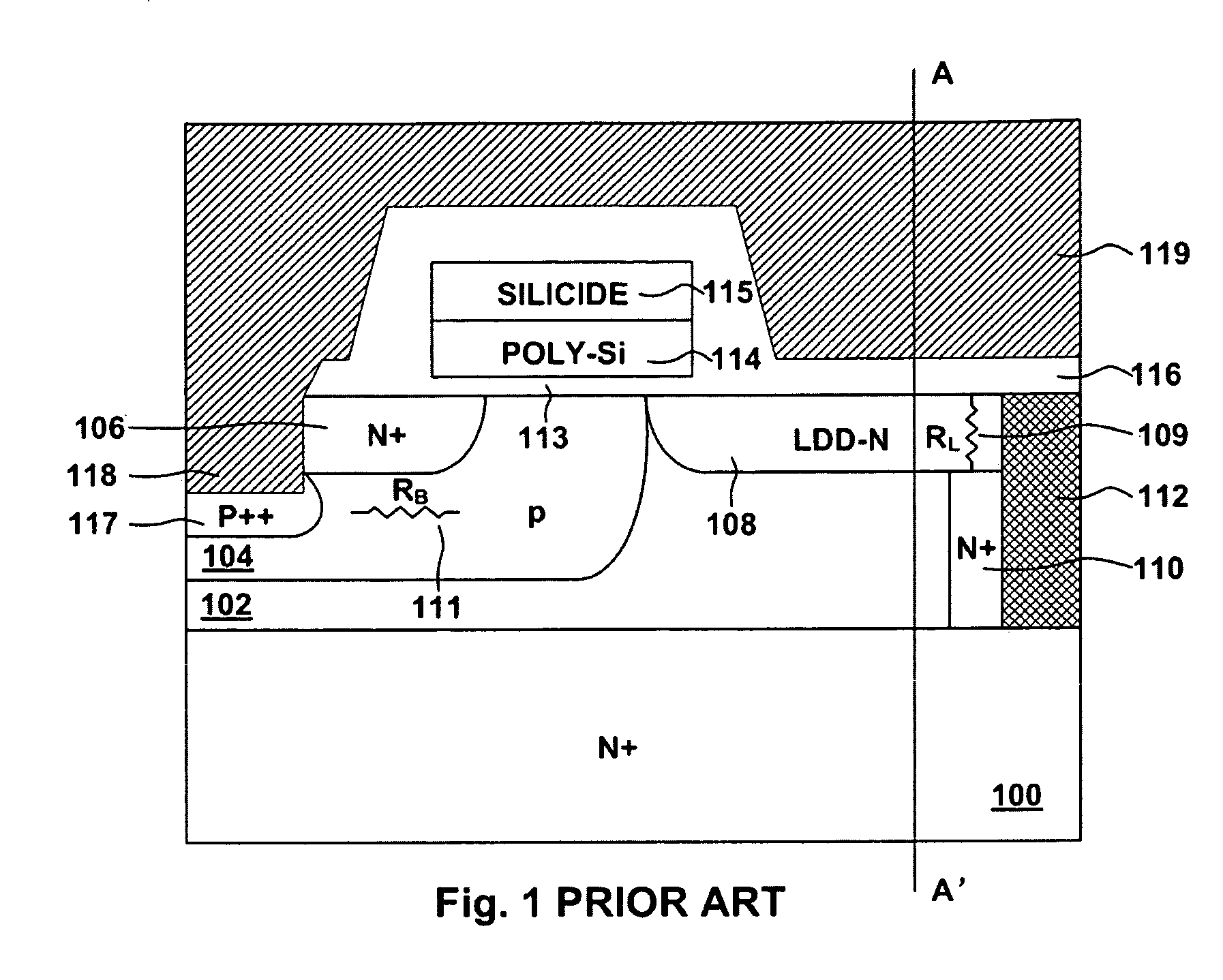
However, the low concentration of drain region can not provide a low resistance path for current flow, that means the on resistance between drain and source (Rdson) is large due to low doping concentration in drain region, which will lead to a large conduction loss.
Another disadvantage of the prior art is that, there is a high parasitic resistance RL109 between surface of the LDD region 108 and N+ region 110 connected to bottom of LDD region 108 due to the lower doping concentration, causing high Rdson between drain and source.
Another disadvantage of the prior is that, a parasitic bipolar N+PN in the prior art is easily triggered on due to existence of high base resistance RB111 underneath source region 106, resulting in device destroy.

Method used


Image

  • LDMOS with double LDD and trenched drain
  • LDMOS with double LDD and trenched drain
  • LDMOS with double LDD and trenched drain

Examples


Embodiment Construction

[0032]Please refer to FIG. 2 for a preferred embodiment of the present invention. The shown LDMOS cell is formed on an N+ substrate 200 onto which grown a P− epitaxial layer 202 wherein P body region 204 is implanted. Source region 206 is formed near the top surface of P body region 204 with a P+ avalanche improved region 217 underneath using the same source mask. Adjacent to LDD-N1 region 208 and LDD-N2 region 209 which is implanted successively near the top surface of epitaxial layer, a first trench is etched through epitaxial layer and filled with doped poly, Ti / TiN / W or Co / TiN / W as drain contact metal plug 212. A highly doped region 210 of N+ doping type is formed next to said drain contact underneath LDD-N1 region to provide a low resistance path for current flow. Above a first insulating layer, which serves as gate oxide layer 213, conductive gate 214 is formed over channel region with a layer of silicide 215 thereon, partially overlaps source region 206, LDD-N1 region 208 and...


PUM


Abstract

A LDMOS with double LDD and trenched drain is disclosed. According to some preferred embodiment of the present invention, the structure contains a double LDD region, including a high energy implantation to form lightly doped region and a low energy implantation thereon to provide a low resistance path for current flow without degrading breakdown voltage. At the same time, a P+ junction made by source mask is provided underneath source region to avoid latch-up effect from happening.

Description

BACKGROUND OF THE INVENTION[0001]1. Field of the Invention[0002]This invention relates generally to the cell structure and fabrication process of power semiconductor devices. More particularly, this invention relates to a novel and improved cell structure and improved process for fabricating a LDMOS (Laterally Diffused MOS transistors) with double LDD (Lightly Doped Drain) and trenched drain structure to provide a low resistance path for the current with enhanced FOM characteristic.[0003]2. The Prior Arts[0004]In U.S. Pat. No. 7,282,765, a LDMOS transistor cell with substrate having a first N semiconductor doping type of prior art was disclosed, as shown in FIG. 1. The transistor cell structure comprises: a highly N+ doped substrate 100 onto which formed a lightly doped epitaxial layer 102 having dopants of N or P dopant type; a body region 104 having P type dopants within which implanted an N+ source region 106; a LDD region 108 formed into epitaxial layer 102 while adjacent to the...

Claims


Application Information

Patent Timeline
Patent Type & Authority Applications(United States)
IPC IPC(8): H01L29/78H01L21/336
CPCH01L21/26586H01L29/0847H01L29/105H01L29/1083H01L29/402H01L29/7835H01L29/41766H01L29/41775H01L29/456H01L29/4933H01L29/66659H01L29/4175
Inventor HSIEH, FU-YUAN
Owner FORCE MOS TECH CO LTD
Learn More