
Field-effect transistor and method of manufacturing the same

a field-effect transistor and field-effect technology, which is applied in the field of field-effect transistors and a manufacturing method of field-effect transistors, can solve the problems of increasing gate capacitance, affecting the performance of field-effect transistors, and general moisture resistance of field-effect transistors using compound semiconductors, so as to achieve high etching resistance and improve moisture resistance. , the effect of high moisture resistan

Inactive Publication Date: 2010-09-02
MITSUBISHI ELECTRIC CORP
View PDF11 Cites 9 Cited by
  • Summary
  • Abstract
  • Description
  • Claims
  • Application Information

AI Technical Summary

Benefits of technology

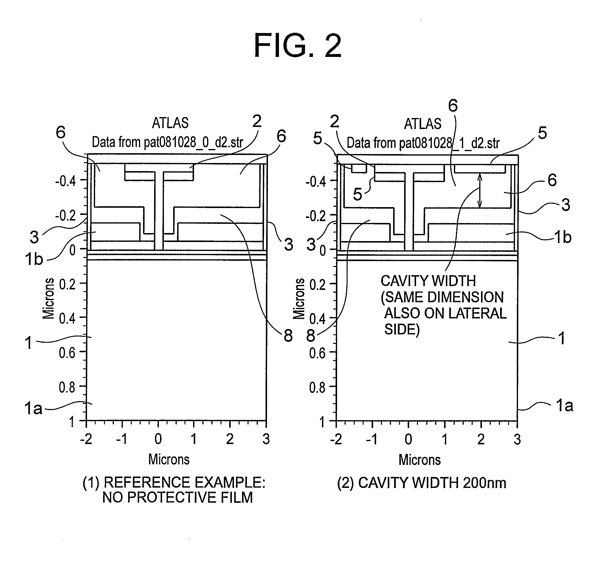
[0013]According to the present invention, by providing the field-effect transistor including: the T-shaped gate electrode formed on the semiconductor layer; and the protective film including one of the insulating film and the organic film having high moisture resistance and high etching resistance, the protective film being formed above the T-shaped gate electrode over the entire transistor active region, which is the region in which the T-shaped gate electrode is formed, in which: the cavity is formed between the semiconductor layer and the protective film in the vicinity of the T-shaped gate electrode, the vicinity including the portion below the canopy of the T-shaped gate electrode; and an end surface of the cavity open to an outside is closed by the highly-moisture-resistant film, the moisture resistance can be improved to a large extent while suppressing the increase in gate capacitance.

Problems solved by technology

Meanwhile, a field-effect transistor using the compound semiconductor is generally vulnerable to moisture, and is required to attain high moisture resistance of a chip itself.
However, in general, the covering by the moisture-resistant protective film accompanies deterioration of transistor characteristics.
In a case of the field-effect transistor, an insulating protective film is interposed in a space between a gate electrode and the surface of the semiconductor or between the gate electrode and source and drain electrodes, and therefore a gate capacitance is increased, with the result that the device characteristics are deteriorated.
However, forming the cavity only below the canopy of the T-shaped gate cannot eliminate a constant increase in gate capacitance due to the highly-moisture-resistant insulating film deposited outside the canopy of the T-shaped gate.
As a result, there arises a problem that a gain reduction is caused.

Method used


Image

  • Field-effect transistor and method of manufacturing the same
  • Field-effect transistor and method of manufacturing the same
  • Field-effect transistor and method of manufacturing the same

Examples


embodiment 1

[0019]Hereinafter, an embodiment of a field-effect transistor and a method of manufacturing the field-effect transistor according to the present invention is described. The field-effect transistor according to the present invention enables large improvement of moisture resistance while suppressing of an increase in gate capacitance, by forming a cavity on a surface of a semiconductor (or on a protective insulating film deposited on the surface) around a gate and in the vicinity thereof including a portion below a canopy of the gate, and by arranging a highly-moisture-resistant protective film thereon.

[0020]FIG. 1 illustrates a structure of a field-effect transistor according to a first embodiment of the present invention. In the field-effect transistor according to the first embodiment of the present invention, as illustrated in FIG. 1, a T-shaped gate electrode 2 and a source or drain (hereinafter, referred to as SD) electrode 3 are formed on a predetermined region defined on a sem...


PUM


Abstract

A field-effect transistor with improved moisture resistance without an increase in gate capacitance, and a method of manufacturing the field-effect transistor are provided. The field-effect transistor includes: a T-shaped gate electrode on a semiconductor layer; and a first highly moisture-resistant protective film including one of an insulating film and an organic film having high etching resistance, the first highly moisture-resistant protective film being located above the T-shaped gate electrodes over all of a region in which the T-shaped gate electrode is located. A cavity is located between the semiconductor layer and the first highly moisture-resistant protective film below a canopy of the T-shaped gate electrode. An end surface of the cavity is closed by a second highly moisture-resistant film.

Description

BACKGROUND OF THE INVENTION[0001]1. Field of the Invention[0002]The present invention relates to a field-effect transistor and a method of manufacturing the field-effect transistor, and more particularly, to a field-effect transistor containing gallium arsenide (GaAs) or gallium nitride (GaN) as a main component, which is suitable for use in a microwave band and a millimeter wave band of several GHz or more, and a method of manufacturing the field-effect transistor.[0003]2. Description of the Related Art[0004]Wireless communication markets using a microwave band and a millimeter wave band are expanding along with the diffusion of satellite communications, high-speed and large-capacity communication systems of a 60 GHz band, on-vehicle radar systems of a 70 to 80 GHz band, and the like. For a transmitting / receiving portion of a signal in those high frequency bands, a field-effect transistor (hereinafter, referred to as FET) such as a metal semiconductor FET (MESFET), a heterostructur...

Claims


Application Information

Patent Timeline
Patent Type & Authority Applications(United States)
IPC IPC(8): H01L29/80H01L21/56H01L23/00
CPCH01L29/0649H01L29/2003H01L29/8128H01L29/7786H01L29/42316
Inventor AMASUGA, HIROTAKA
Owner MITSUBISHI ELECTRIC CORP
Learn More