Substrate processing apparatus
- Summary
- Abstract
- Description
- Claims
- Application Information
AI Technical Summary
Benefits of technology
Problems solved by technology
Method used
Image
Examples
Embodiment Construction
(1) Structure of a Substrate Processing Apparatus
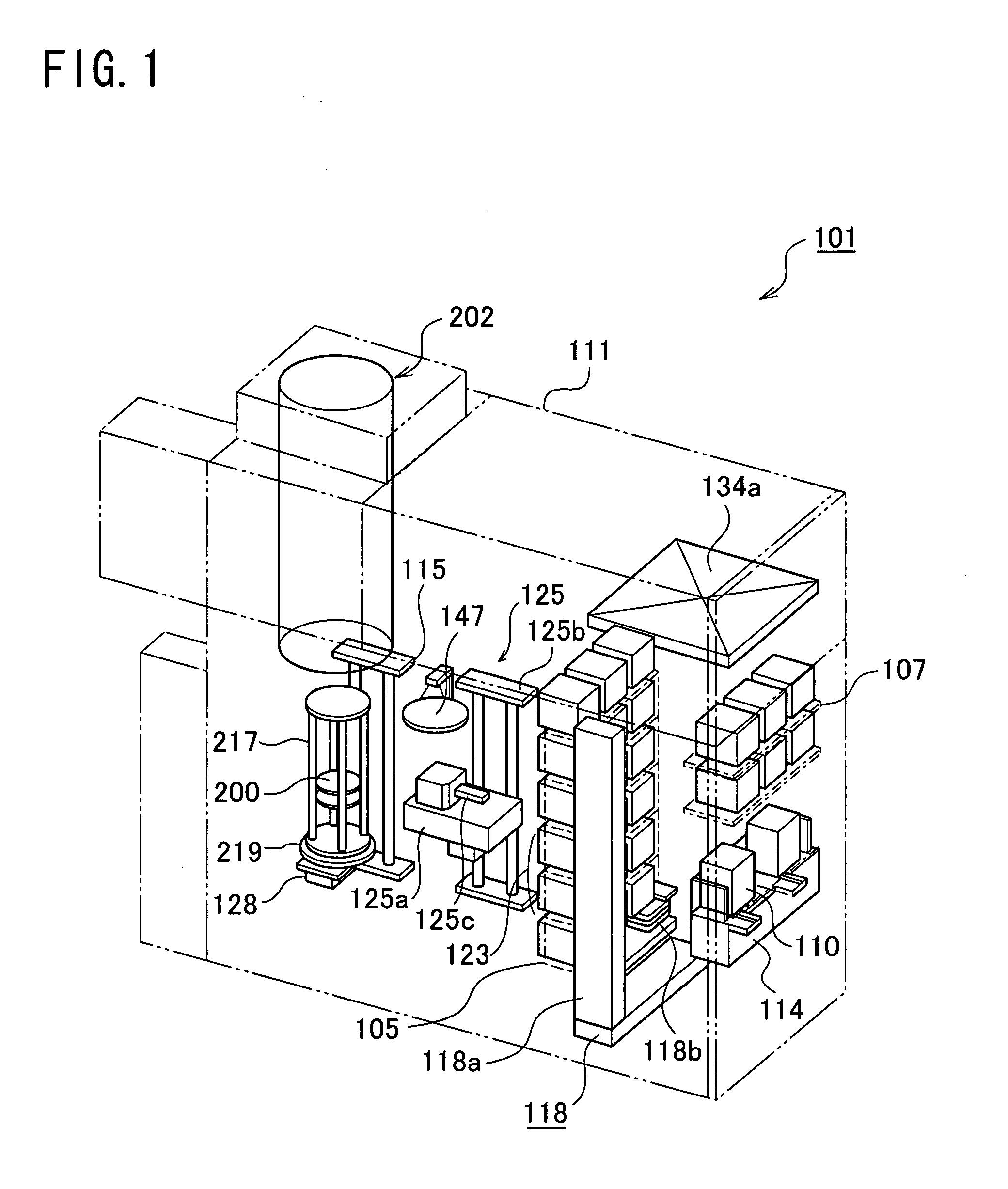
[0020]First, a structural example of a substrate processing apparatus 101 according to an embodiment of the present invention will be described, by using FIG. 1.
[0021]As shown in FIG. 1, the substrate processing apparatus 101 according to this embodiment includes a casing 111. In order to carry a wafer (substrate) 200 configurated to silicon to inside / outside of the casing 111, a cassette 110 is used, being a wafer carrier (substrate storage container) for storing a plurality of wafers 200. A cassette stage (substrate storage container transfer stand) 114 is provided on the front side of the casing 111 (right side in the figure). The cassette 110 is placed on the cassette stage 114 by an in-step carrying device not shown, and is unloaded to outside of the casing 111 from the cassette stage 114.
[0022]The cassette 110 is placed on the cassette stage 114, so that the wafer 200 in the cassette 110 is set in a vertical posture, and a wafer...
PUM
| Property | Measurement | Unit |
|---|---|---|
| Length | aaaaa | aaaaa |
| Volume | aaaaa | aaaaa |
| Area | aaaaa | aaaaa |
Abstract
Description
Claims
Application Information
 - R&D
- Intellectual Property
- Life Sciences
- Materials
- Tech Scout
- Unparalleled Data Quality
- Higher Quality Content
- 60% Fewer Hallucinations
Browse by: Latest US Patents, China's latest patents, Technical Efficacy Thesaurus, Application Domain, Technology Topic, Popular Technical Reports.
© 2025 PatSnap. All rights reserved.Legal|Privacy policy|Modern Slavery Act Transparency Statement|Sitemap|About US| Contact US: help@patsnap.com


