
Mask inspection apparatus and image creation method

a mask inspection and mask technology, applied in the field of mask inspection apparatus and image creation method, can solve the problems of low exposure precision, patterns cannot be transferred to desired positions, and patterns may be transferred incorrectly,

Inactive Publication Date: 2010-08-05
ADVANTEST CORP
View PDF3 Cites 9 Cited by
  • Summary
  • Abstract
  • Description
  • Claims
  • Application Information

AI Technical Summary

Benefits of technology

[0017]According to the invention, an image of a wide field of view corresponding to the designated observation area is acquired in the following way. Firstly, the designated observation area of the sample is divided into plural divisional areas so that the adjacent divisional areas partially overlap each other. Then, a high-precision image is acquired for each of the divisional areas. After that, the images of all the divisional areas are synthesized on the basis of the coordinate data for each divisional area and of the edge information for each pattern formed in each of the portions where adjacent divisional areas overlap each other. Accordingly, it is possible to create a high-precision sample image even if the image must cover a wide field of view.

Problems solved by technology

If the patterns formed on the photomask have any defects or distortions, such defects or distortions may result in lower exposure precision.
For example, the patterns cannot be transferred to desired positions, or the shapes of the patterns may be transferred incorrectly.
In addition, if a wide field of view is scanned by an ordinary critical dimension SEM, various kinds of aberrations such as the astigmatism, the field curvature, and the distortion inevitably take place.
The dynamic and simultaneous correction imposes a heavy load on the mask-inspection apparatus, or worse yet, the correction can be done imperfectly.
Nevertheless, when the sample stage is moved so as to take an image of a particular divisional area, the movement of the sample stage is not always as precise as required.
Hence, even when a series of photos to be joined are taken, the photos cannot necessarily be synthesized successfully into a perfect single-piece photo of a wide field of view.

Method used


Image

  • Mask inspection apparatus and image creation method
  • Mask inspection apparatus and image creation method
  • Mask inspection apparatus and image creation method

Examples


Embodiment Construction

[0031]Some embodiments of the invention will be described below by referring to the drawings.

[0032]To begin with, a description will be given as to the configuration of a scanning electron microscope to be used as a mask inspection apparatus. Then, a description will be given as to how to measure the size of a pattern using a common SEM image. After that, a description will be given as to how to acquire a high-precision SEM image that covers a wide field of view.

(Configuration of Scanning Electron Microscope)

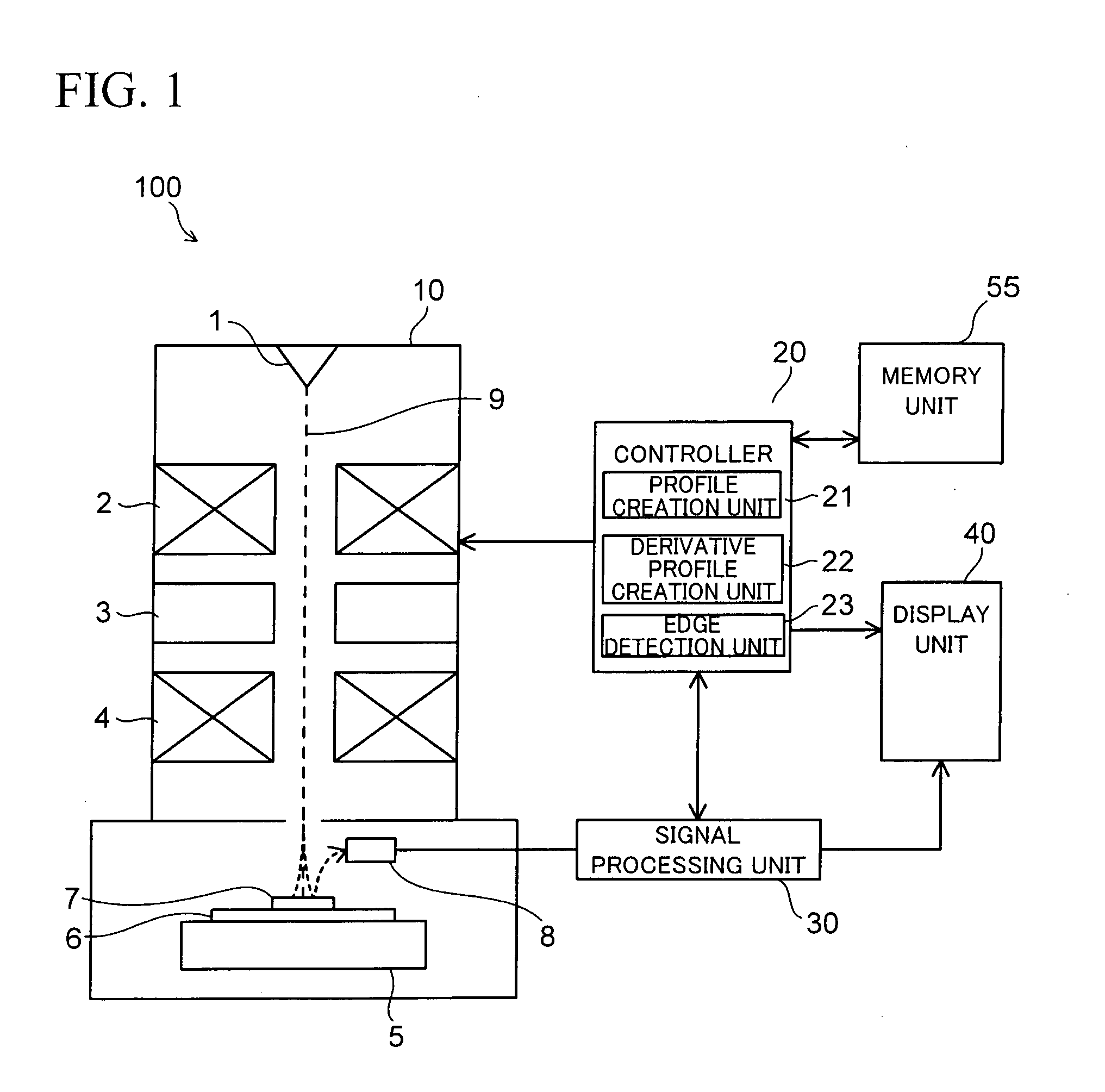
[0033]FIG. 1 is a diagram illustrating the configuration of a scanning electron microscope according to this embodiment.

[0034]This scanning electron microscope 100 is roughly divided into an electron scanning unit 10, a signal processing unit 30, a display unit 40, a memory unit 55, and a controller 20. The controller 20 controls the electron scanning unit 10, the signal processing unit 30, the display unit 40, and the memory unit 55. The controller 20 includes a profile creatio...


PUM

PropertyMeasurementUnit
image processingaaaaaaaaaa
sizeaaaaaaaaaa
SEMaaaaaaaaaa

Abstract

Provided is a mask inspection apparatus including: emitting unit for emitting electron beams onto a sample; electron detecting unit for detecting the quantity of electrons produced, by the emission of the electron beams, from the sample with patterns formed thereon; image processing unit for generating image data for the patterns on the basis of the electron quantity; and controlling unit for controlling the emitting unit, the electron detecting unit, and the image processing unit. The controlling unit calculates, from the size of a designated observation area of the sample, a division number of divisional images that are synthesized to form a joint image that covers the entire designated observation area. The controlling unit determines divisional areas so that adjacent divisional areas partially overlap each other. The controlling unit acquires SEM images for the respective divisional areas. The controlling unit synthesizes the SEM images of the divisional areas on the basis of coordinate data for the divisional areas and on the basis of edge information for patterns included in the overlapping regions, and thereby creates an SEM image of a wide field of view that covers the observation area.

Description

[0001]This application claims the benefit of U.S. Provisional Patent Application Ser. No. 61 / 206,821 filed Feb. 4, 2009, all of which are hereby incorporated by reference.BACK GROUND OF THE INVENTION[0002]1. Field of the Invention[0003]The invention relates to a mask inspection apparatus and an image creation method which are capable of creating an image of a wide field of view and of a high resolution.[0004]2. Description of the Prior Art[0005]In a lithography process of semiconductor manufacturing processes, patterns formed on a photomask is exposed to light by an exposure apparatus and is transferred onto a wafer. If the patterns formed on the photomask have any defects or distortions, such defects or distortions may result in lower exposure precision. For example, the patterns cannot be transferred to desired positions, or the shapes of the patterns may be transferred incorrectly. To prevent the decrease in the exposure precision, the photomask is inspected to check whether or n...

Claims


Application Information

Patent Timeline
Patent Type & Authority Applications(United States)
IPC IPC(8): G03F1/00G01N23/00
CPCG03F1/86G03F1/0092
Inventor MURAKAWA, TSUTOMUIWAI, TOSHIMICHIMATSUMOTO, JUNNAKAMURA, TAKAYUKIOGISO, YOSHIAKI
Owner ADVANTEST CORP
Learn More