Sensors using high electron mobility transistors
a high electron mobility, transistor technology, applied in semiconductor devices, instruments, material electrochemical variables, etc., can solve the problems of limiting the frequency of screening, high patient cost, and invasive radiation, and achieve the effect of facilitating rapid analysis of results
- Summary
- Abstract
- Description
- Claims
- Application Information
AI Technical Summary
Benefits of technology
Problems solved by technology
Method used
Image
Examples
example 1
Selective Detection of Hg(II) Ions from Cu(II) and Pb(II)
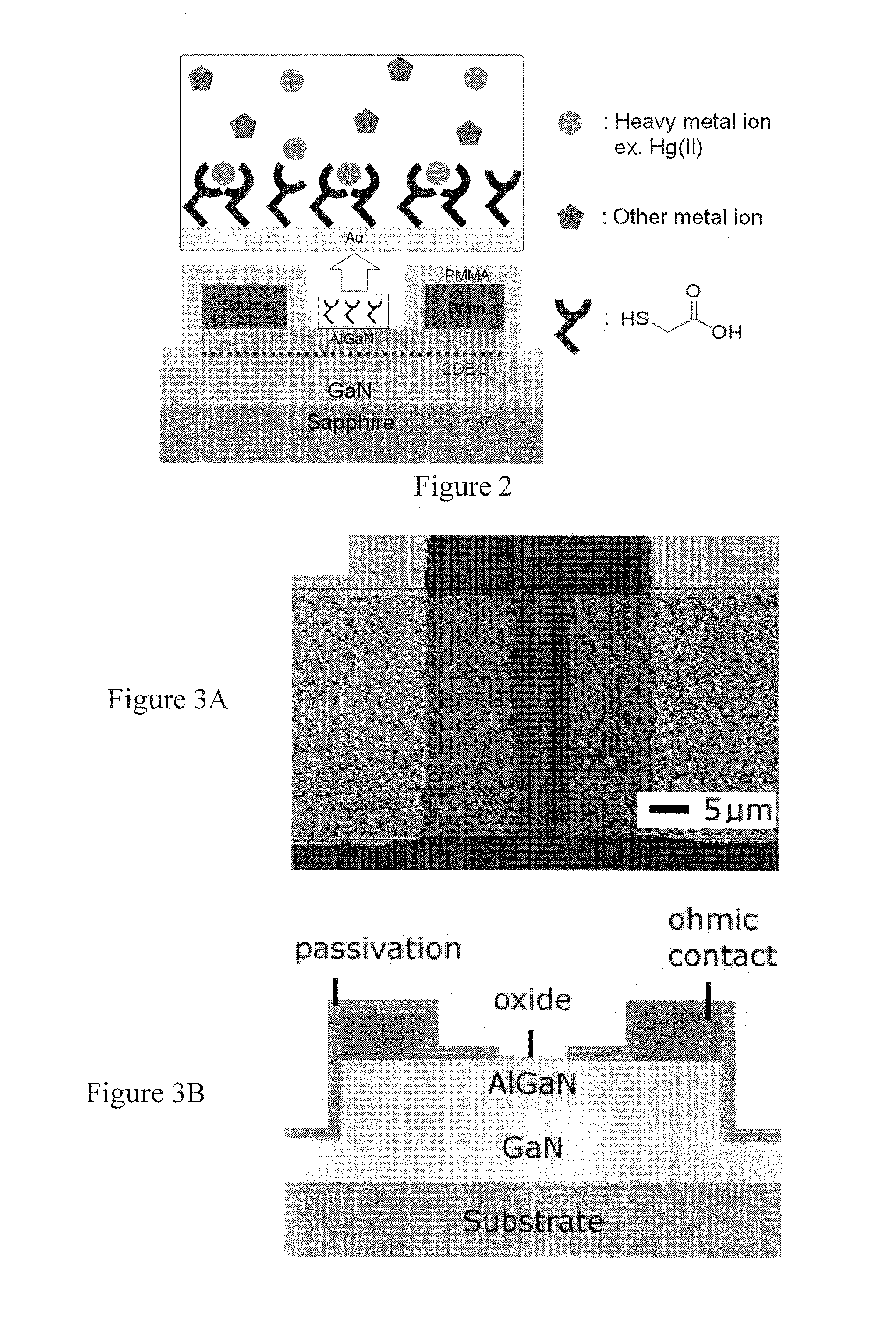
[0088]Hg2+ and Cu2+ ions are easily detected with sensors fabricated with Au-gated and thioglycolic acid functionalized Au-gated GaN / AlGaN HEMTs.
[0089]The HEMT structures consisted of a 2 μm thick undoped GaN buffer and 250 Å thick undoped Al0.25Ga0.75N cap layer. The epi-layers were grown by molecular beam epitaxy system on 2″ sapphire substrates at SVT Associates. Mesa isolation was performed with an Inductively Coupled Plasma (ICP) etching with Cl2 / Ar based discharges at −90 V dc self-bias, ICP power of 300 W at 2 MHz, and a process pressure of 5 mTorr. Ohmic contacts of 50×50 μm2 separated with gaps of 10, 20, and 50 μm were formed by e-beam deposition of Ti / Al / Pt / Au patterns by lift-off and annealed at 850° C. for 45 sec under flowing N2 for source and drain metal contacts. A 5-nm thin gold film was deposited as the gate metal for two sets of sample sensors. One sensor had a bare Au-gate and the other sensor had an Au-gat...
example 2
Detection of Prostate Specific Antigen
[0097]Functionalized of Au-gated AlGaN / GaN HEMTs of the invention were used to detect prostate specific antigen (PSA). The PSA was specifically recognized through PSA antibody, anchored to the gate area in the form of carboxylate succinimidyl ester. A wide range of concentrations from to 1 μg / ml to 10 pg / ml of PSA was investigated, which is lower than the cut-off value of 2.5 ng / ml that is used as an indication for the need of biopsy.
[0098]The HEMT structures consisted of a 3 μm thick undoped GaN buffer, a 30 Å thick Al0.3Ga0.7N spacer, and a 220 Å thick Si-doped Al0.3Ga0.7N cap layer. Epi-layers were grown by rf plasma-assisted Molecular Beam Epitaxy on the thick GaN buffers produced on sapphire substrates by metal organic chemical vapor deposition (MOCVD). Mesa isolation was performed with an Inductively Coupled Plasma (ICP) etching with Cl2 / Ar based discharges at −90 V dc self-bias, ICP power of 300 W at 2 MHz, and a process pressure of 5 mTo...
example 3
Detection of Changes in pH in Electrolyte Solutions
[0105]A Sc2O3 gate dielectric on AlGaN / GaN HEMTs is shown to provide high sensitivity for detecting changes in pH of electrolyte solutions, and is superior to the use of native oxide in the gate region.
[0106]The HEMT structures consisted of a 2 μm thick undoped GaN buffer and 250 Å thick undoped Al0.25Ga0.75N cap layer. The epi-layers were grown by Metal-Organic Chemical Vapor Deposition on 100 mm (111) Si substrates at Nitronex Corporation. The sheet carrier concentration was ˜1×1013 cm−2 with a mobility of 980 cm2 / V-s at room temperature. Mesa isolation was achieved by using an ICP system with Ar / Cl2 based discharges. Ohmic contacts of 50×50 μm2 separated with gaps of 10, 20, and 50 μm were formed by lift-off of e-beam deposited Ti(200 Å) / Al(800 Å) / Pt(400 Å) / Au(800 Å). The contacts were annealed at 850° C. for 45 sec under a flowing N2 ambient in a Heatpulse 610T system. A 100 Å Sc2O3 layer was deposited as a gate dielectric throu...
PUM
| Property | Measurement | Unit |
|---|---|---|
| concentrations | aaaaa | aaaaa |
| thick | aaaaa | aaaaa |
| contact angle | aaaaa | aaaaa |
Abstract
Description
Claims
Application Information
 - R&D
- Intellectual Property
- Life Sciences
- Materials
- Tech Scout
- Unparalleled Data Quality
- Higher Quality Content
- 60% Fewer Hallucinations
Browse by: Latest US Patents, China's latest patents, Technical Efficacy Thesaurus, Application Domain, Technology Topic, Popular Technical Reports.
© 2025 PatSnap. All rights reserved.Legal|Privacy policy|Modern Slavery Act Transparency Statement|Sitemap|About US| Contact US: help@patsnap.com


