Optimizing Sram Performance over Extended Voltage or Process Range Using Self-Timed Calibration of Local Clock Generator

a local clock generator and voltage or process range technology, applied in the field of clock or timing circuits, can solve the problems of increasing the prevalence of low power circuits, large number of cells, and complicated connections between cells, and achieve the effect of improving the clock generation circui

Inactive Publication Date: 2010-04-08
GLOBALFOUNDRIES INC
View PDF11 Cites 15 Cited by
  • Summary
  • Abstract
  • Description
  • Claims
  • Application Information

AI Technical Summary

Benefits of technology

[0015]It is yet another object of the present invention to provide a method of optimizing SRAM performance over an extended voltage or process range using self-timed calibration of a local clock.

Problems solved by technology

An IC may include a very large number of cells and require complicated connections between the cells.
Low power circuits are becoming more prevalent due to power consumption problems.
Excess power usage is not only costly and inefficient, but also leads to heat management problems.
Power dissipation has become a limiting factor for the yield of high-performance circuit designs (operating at frequencies around 1 gigahertz or more) with deep submicron technology.
The power constraint thus presents an additional challenge for the designer in constructing a clock network for the cells, and this challenge is becoming more difficult with the latest technologies like low-power, 65-nanometer integrated circuits.
The use of different voltages for different cells in a circuit combined with dynamic voltage scaling presents unique problems, especially with low voltage operations, since the delays of different cells scale differently at low voltages.
This delay differential can be significant, negatively impacting manufacturing requirements and / or circuit performance.
However, it is very difficult to control this timing component with dynamic voltage scaling because of variations in inverter delay with changes in supply voltage and differences between threshold voltages.
While the number of delay elements may be selectively programmed with this circuit, there are still variations in the actual delay of these elements with respect to supply voltage which are only imprecisely known, so this approach is not feasible for devices that are particularly sensitive at low voltages.
While this approach provides a real-time basis for delay adjustment, the delay variation of the replicated SRAM path may not match the delay variation in the LCB logic as explained above, resulting in poor timing control.

Method used


Image

  • Optimizing Sram Performance over Extended Voltage or Process Range Using Self-Timed Calibration of Local Clock Generator
  • Optimizing Sram Performance over Extended Voltage or Process Range Using Self-Timed Calibration of Local Clock Generator
  • Optimizing Sram Performance over Extended Voltage or Process Range Using Self-Timed Calibration of Local Clock Generator

Examples


Embodiment Construction

)

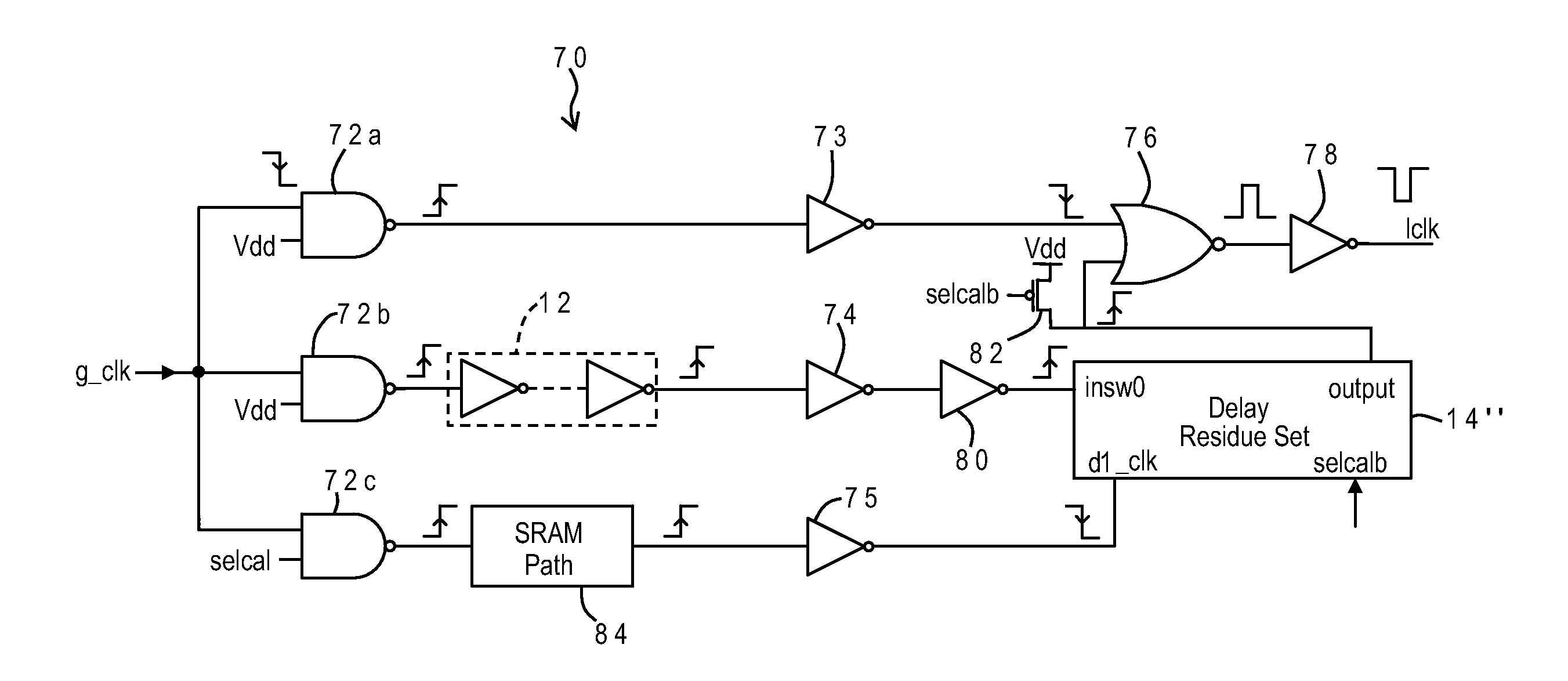
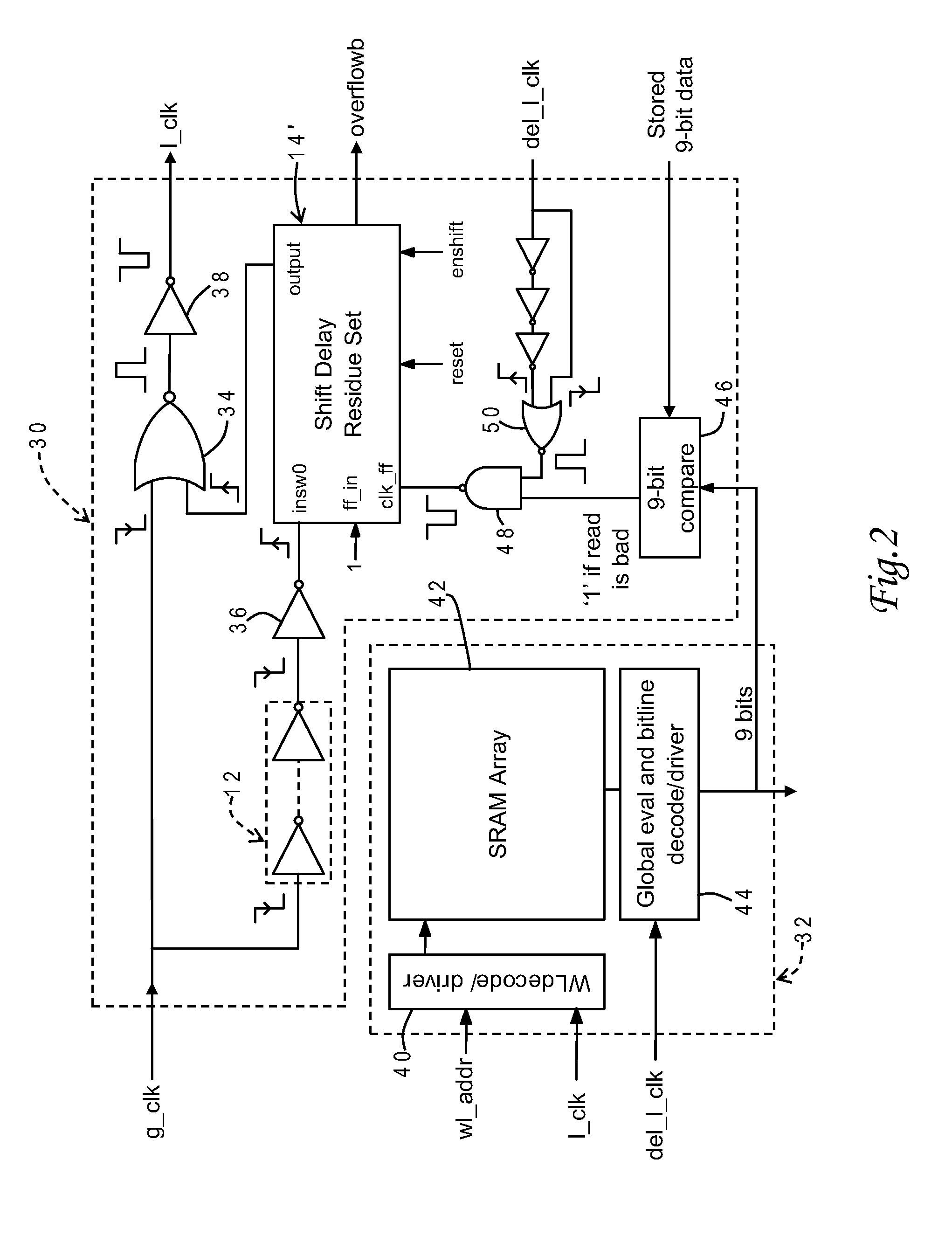
[0028]The present invention is directed to improved methods and integrated circuit structures for generating timing or clock signals. In particular the invention is applicable to timing control for circuit components which use local clock signals and a delayed clock signal, such as a static, random-access memory (SRAM) array. The invention provides precise adjustment of the delayed clock signal to optimize SRAM performance over an extended range of operational, process or environmental parameters.

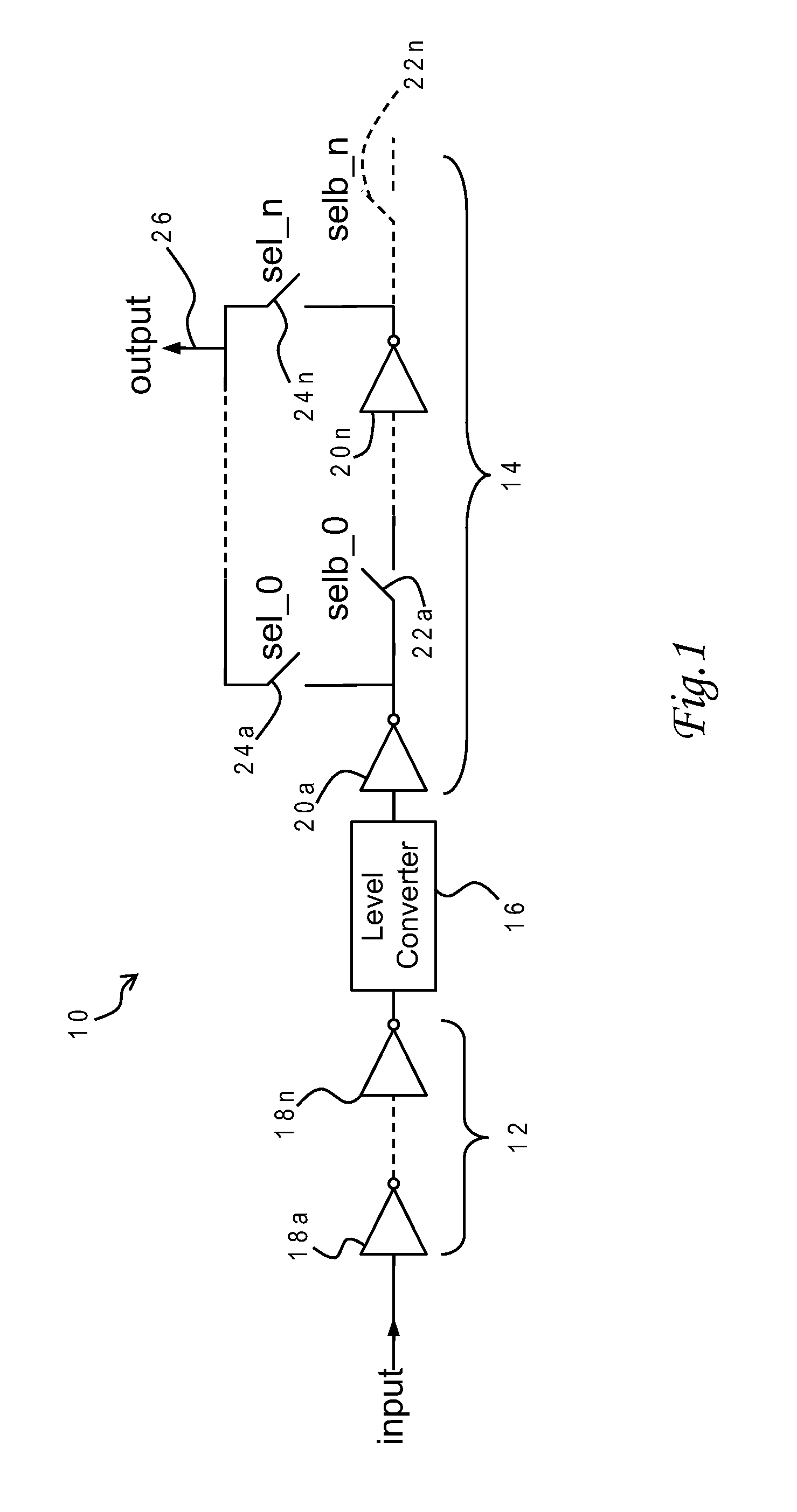
[0029]With reference now to the figures, and in particular with reference to FIG. 1, there is depicted one embodiment 10 of a delay circuit constructed in accordance with the present invention. Delay circuit 10 is generally comprised of an inverter chain 12 having a fixed length, a linear programmable delay residue 14 whose delay is selectively adjusted, and a level converter 16 interconnecting fixed inverter chain 12 to linear programmable delay residue 14. Inverter chain 12 includes a fi...


PUM


Abstract

A delay circuit has a fixed delay path at a lower voltage level, a level converter, and an adjustable delay path at a higher voltage level. The fixed delay path includes an inverter chain, and the adjustable delay path includes serially-connected delay elements selectively connected to the circuit output. In an application for a local clock buffer of a static, random-access memory (SRAM), the lower voltage level is that of the local clock buffer, and the higher voltage level is that of the SRAM. These voltages may vary in response to dynamic voltage scaling, requiring re-calibration of the adjustable delay path. The adjustable delay path may be calibrated by progressively increasing the read access time of the SRAM array until a contemporaneous read operation returns the correct output, or by using a replica SRAM path to simulate variations in delay with changes in voltage supply.

Description

BACKGROUND OF THE INVENTION[0001]1. Field of the Invention[0002]The present invention generally relates to clock or timing circuits, and more particularly to a method of operating a memory array such as static, random-access memory (SRAM) which uses locally generated clock signals.[0003]2. Description of the Related Art[0004]Integrated circuits are used for a wide variety of electronic applications, from simple devices such as wristwatches to the most complex computer systems. A microelectronic integrated circuit (IC) chip can generally be thought of as a collection of logic cells with electrical interconnections between the cells, formed on a semiconductor substrate (e.g., silicon). An IC may include a very large number of cells and require complicated connections between the cells. A cell is a group of one or more circuit elements such as transistors, capacitors, resistors, inductors, and other basic circuit elements grouped to perform a logic function. Cell types include, for exa...

Claims


Application Information

Patent Timeline
Patent Type & Authority Applications(United States)
IPC IPC(8): G11C7/00G11C8/18H03H11/26H03K3/00H03L5/00G11C8/08
CPCG11C7/22G11C11/419G11C11/417G11C11/413
Inventor CARPENTER, GARY D.KUANG, JENTE B.NOWKA, KEVIN J.PANG, LIANG-TECK
Owner GLOBALFOUNDRIES INC
Why Eureka
Try Eureka