Reverse x-ray photoelectron holography device and its measuring method

a photoelectron and holography technology, applied in the direction of instruments, x/gamma/cosmic radiation measurement, material analysis using wave/particle radiation, etc., can solve the problems of inability to measure a large number of test samples, inability to readily available, and limited measurement time, so as to achieve high-precision atomic images, easy detection of characteristic x-rays, and extreme ease of measurement

Inactive Publication Date: 2010-03-25
JAPAN SYNCHROTRON RADIATION RES INST +1
View PDF4 Cites 8 Cited by
  • Summary
  • Abstract
  • Description
  • Claims
  • Application Information

AI Technical Summary

Benefits of technology

[0022]With the inverse X-ray photoelectron holography device according to the present invention, the accelerating voltage can be varied to measure holograms having a plurality of wavelengths, and highly precise atomic images can be reproduced from a plurality of holograms having numerous wavelengths due to the use of an electron beam instead of X-rays.
[0023]The contrast of a fluorescent X-ray hologram obtained using X-ray interference has an amplitude that is about 0.1% less than the background intensity. However, a hologram obtained by inverse X-ray photoelectron holography, which measures electron interference patterns, has the advantage of extreme ease of measurement because the contrast is about 1 to 10%.
[0024]A device which uses an electron beam has the further advantage of being able to easily detect characteristic X-rays from a X-ray element being released because the operation must always be conducted in a vacuum.
[0025]Microcrystals, materials, and other items in which the samples to be measured are several microns or less in size can be measured by applying the present invention to a commercially available scanning electron microscope or transmission electron microscope and ensuring convergence of an electron beam to a size of several microns or less. The advantages are that the ease of use is improved in comparison with conventional measurement devices and that atomic images can be easily analyzed inside laboratories without the use of large-scale facilities.

Problems solved by technology

Because many such facilities are public facilities, there are many cases in which they are not readily available.
Also, when using the facilities, the time available for measurements is often limited and it is not possible to measure a large number of test samples.
Because about two months, which is more than approximately a few weeks, was required, there was a large burden on researchers.
However, this device had the disadvantages that the wavelength could not be freely varied since a rotating-anticathode X-ray generator was used, and that a sharp atomic image could not be obtained or the measurable samples were limited since sufficiently intense X-rays could not be obtained.
Although many dopants of semiconductors or the like are nitrogen, phosphorus, and other X-ray elements (elements having an atomic number lower than that of Ca), measuring the fluorescent X-rays of X-ray elements in the atmosphere is difficult due to air absorption, and holograms focusing on these atoms cannot be measured.
Collecting X-rays is difficult in cases in which the X-rays are used as an excitation source, and microcrystals or the like several microns in size cannot be used as measurement objects.
As stated above, since X-rays were used as an excitation source in conventional devices, energy control and convergence was difficult to accomplish, and holograms having good contrast could not be obtained.
Even when large-scale facilities were used, the devices were restricted in a variety of ways and were not easy to use.

Method used


Image

  • Reverse x-ray photoelectron holography device and its measuring method
  • Reverse x-ray photoelectron holography device and its measuring method
  • Reverse x-ray photoelectron holography device and its measuring method

Examples


Embodiment Construction

[0034]Embodiments of the present invention will be described in detail hereinafter with reference to the annexed drawings.

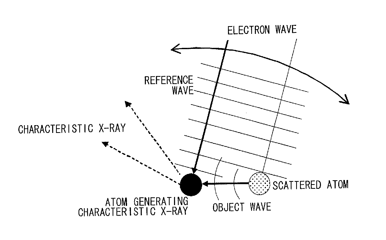
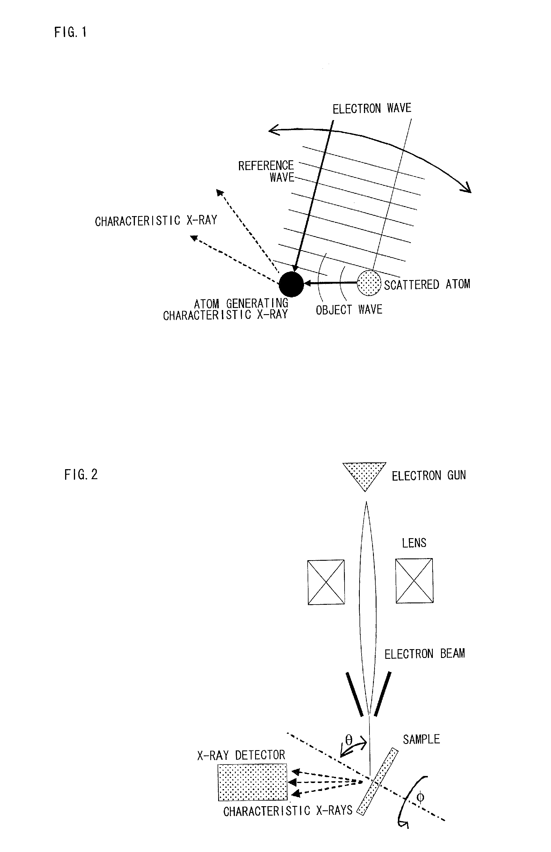
[0035]FIG. 1 shows the principle of inverse X-ray photoelectron holography. An embodiment of the present invention will be described using FIG. 1. Electrons (waves) are directed toward atoms that constitute a structure characteristic of the solid in a solid measurement sample from an electron gun by using a inverse X-ray photoelectron holography device or the like. The electrons are made to strike and excite the measurement sample, and characteristic X-rays are generated by the atoms that constitute the structure of the measurement sample. Because of the phenomenon in which the electrons arrive directly without being scattered by other atoms when the characteristic X-rays are generated, the electron wave in holography formed in this manner is considered to be a reference wave.

[0036]Next, a phenomenon occurs in which an electron wave that has caused a single cycle...


PUM


Abstract

[Problems] To provide a reverse X-ray photoelectron holography device, in which energy control and convergence are facilitated and a hologram of good contrast is obtained; and to provide its measuring method.[Means for Solving Problems] A Reverse X-ray photoelectron holography measuring method where a measurement sample is irradiated with an electron beans, incident angle and rotation angle of the electron beam are varied by varying the posture of the measurement sample to the electron beam, and a variation in intensity of characteristic X-ray emitted when the measurement sample is excited is recorded as the atomic resolution hologram around the atom of a specific element, wherein, when the intensity is detected as the characteristic X-ray of the atom of the measurement sample, an object wave is generated as an electron wave scattered by the reference wave and the proximity atom in a holography where electrons incident to the measurement sample reach an atom generating specific X-ray as an electron wave, and an interference pattern is formed by compounding the reference wave with the object wave, thus monitoring the intensity of an electron beam.

Description

TECHNICAL FIELD[0001]The present invention relates to a inverse X-ray photoelectron holography measurement device for irradiating a measurement sample with an electron beam, detecting the intensity distribution pattern of an emitted characteristic X-ray, and using a Fourier transform to acquire an image, and also relates to a measurement method thereof.BACKGROUND ART[0002]X-ray photoelectron holography and fluorescent X-ray holography techniques are effective in determining the crystalline structure of miniaturized electronic devices or thin-film materials and other industrial materials, evaluating crystalline properties, and analyzing local structures and structural changes due to temperature variations and chemical variations, and involve obtaining three-dimensional images of structures of the environment on the atomic level around an atom of a specific element. These techniques are currently providing important knowledge in explaining the functions of advanced materials, such as ...

Claims


Application Information

Patent Timeline
IPC IPC(8): G01N23/223G01B15/04
CPCG01N23/2252G03H5/00G01N2223/079
Inventor HAYASHI, KOICHIMATSUBARA, EIICHIROMATSUSHITA, TOMOHIRO
Owner JAPAN SYNCHROTRON RADIATION RES INST
Why Eureka
Try Eureka