
Nitride semiconductor light emitting device and method of manufacturing the same

a light-emitting device and semiconductor technology, applied in semiconductor/solid-state device manufacturing, semiconductor devices, electrical equipment, etc., can solve the problems of difficult to increase the size of the chip, easy deterioration of the chip, and uneven light intensity, and achieve excellent internal quantum efficiency, light extraction efficiency and driving voltage.

Active Publication Date: 2010-02-11
XIAMEN SANAN OPTOELECTRONICS CO LTD
View PDF6 Cites 129 Cited by
  • Summary
  • Abstract
  • Description
  • Claims
  • Application Information

AI Technical Summary

Benefits of technology

[0013]The present invention has been proposed in consideration of the aforementioned problems, and an object thereof is to provide a nitride semiconductor light-emitting device capable of employing a vertical electrode structure and excellent in internal quantum efficiency, light extraction efficiency and driving voltage as well as in mass productivity and a method of manufacturing the same.
[0024]According to the present invention, a nitride semiconductor light-emitting device of a vertical electrode structure or a one-side two-electrode structure excellent in internal quantum efficiency, light extraction efficiency and driving voltage as well as in mass productivity can be provided.

Problems solved by technology

In the nitride semiconductor light-emitting device having such a one-side two-electrode structure, however, the electrodes are not formed on symmetrical positions of the upper and lower surfaces of the chip, and hence luminous intensity is not uniformized in plane, but emission concentrates on the p-side electrode or the n-side electrode.
Further, it is difficult to increase the size of the chip and the chip is easily deteriorated by aging due to the aforementioned problem.
In addition, the pad electrodes provided on one surface occupy large ratios in the surface area of the chip, and it is also difficult to reduce the size of the chip.
In the nitride semiconductor light-emitting device described in this document, however, light extraction efficiency is inferior due to low reflectance of the electrode.
In this structure, however, the light extraction efficiency is not sufficiently improved due to large light absorption by the contact metal such as Ni / Au.
Further, while light absorption by ITO is negligible when the thickness of the DBR layer is about 300 nm, the light extraction efficiency may be insufficiently improved due to large light absorption if a thick film such as a multilayer film is prepared from ITO in order to form the DBR layer.
While this document discloses no specific method of preparing the DBR layer from ITO, it is difficult to increase refractive index difference if a low refractive index layer is made of a material identical to that for a high refractive index layer, and the reflectance of the DBR layer made of ITO cannot be increased as a result.
Further, two electrodes must be formed on one side in this structure, to result in problems identical to the above.
However, both of GaN and SiN are extremely high-priced and not suitable for a low-priced LED.
In order to form the DBR by a multilayer structure of GaN and AlGaN formable by epitaxy on the GaN or SiN substrate, the layers must be extremely multicyclically grown due to small refractive index difference, and it is difficult to construct the DBR due to cracking or the like.
In addition, the quality of an active layer grown on such a DBR is so inferior that internal quantum efficiency is reduced.
When the welding is performed without employing an adhesive, however, the surfaces of both wafers must indispensably be planar, and the wafer bonding cannot be performed if the surface of either wafer is slightly irregularized.
In the case of an actual nitride semiconductor, waste or the like coming off a reactor frequently adheres to the surface of an epiwafer during epitaxy, and it is difficult to completely remove waste from the wafer.
However, it is difficult to prepare a DBR from a nitride semiconductor as hereinabove described, and even if such a DBR can be prepared, no current is injected into a DBR region due to high resistance, and an injection area is reduced.
Consequently, the current density is increased to reduce luminous efficiency.
If Ag is employed as the material for the ohmic contact layer, electromigration takes place to cause a short circuit upon migration to an n side, and hence this structure is extremely problematic in reliability.
As hereinabove described, there has hitherto been implemented no nitride semiconductor light-emitting device excellent in internal quantum efficiency, light extraction efficiency and driving voltage as well as in mass productivity.

Method used


Image

  • Nitride semiconductor light emitting device and method of manufacturing the same
  • Nitride semiconductor light emitting device and method of manufacturing the same
  • Nitride semiconductor light emitting device and method of manufacturing the same

Examples


first embodiment

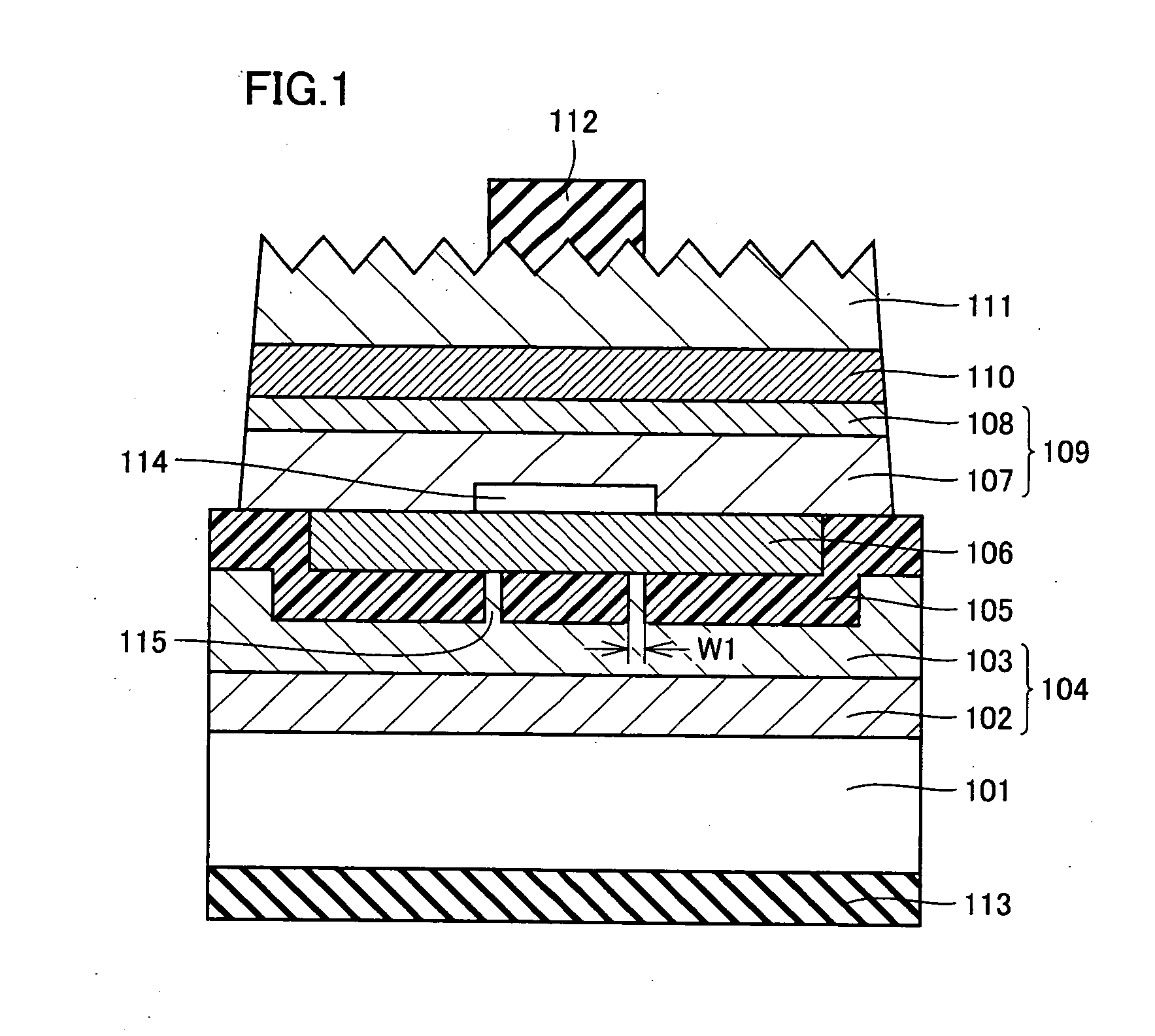
[0031]FIG. 1 is a schematic sectional view showing a first embodiment of a nitride semiconductor light-emitting device according to the present invention. The nitride semiconductor light-emitting device shown in FIG. 1 has a multilayer structure obtained by stacking a support substrate 101; a eutectic bonding layer 104 consisting of a second bonding layer 102 and a first bonding layer 103; a reflecting layer 105 made of dielectric materials; a transparent conductive layer 106; a p-type nitride semiconductor layer 109 consisting of a p-type GaN layer 107 and a p-type AlGaN layer 108; a light emitting layer 110; and an n-type nitride semiconductor layer 111 made of n-GaN in this order. A first electrode (n-side electrode) 112 is formed on the n-type nitride semiconductor layer 111 while a second electrode (p-side electrode) 113 is formed on a surface of the support substrate 101 opposite to the eutectic bonding layer 104, so that the nitride semiconductor light-emitting device has a v...

second embodiment

[0058]FIG. 8 is a schematic sectional view showing a second embodiment of a nitride semiconductor light-emitting device according to the present invention. The nitride semiconductor light-emitting device shown in FIG. 8 is different from the nitride semiconductor light-emitting device shown in FIG. 1 in a point employing a plating underlayer 803 and a plating layer 801 in place of the eutectic bonding layer 104, the support substrate 101 and the second electrode 113 in the nitride semiconductor light-emitting device shown in FIG. 1. In other words, the nitride semiconductor light-emitting device shown in FIG. 8 has a multilayer structure obtained by stacking the plating layer 801; the plating underlayer 803; a reflecting layer 805 made of dielectric materials; a transparent conductive layer 806; a p-type nitride semiconductor layer 809 consisting of a p-type GaN layer 807 and a p-type AlGaN layer 808; a light emitting layer 810; and an n-type nitride semiconductor layer 811 made of ...

example 1

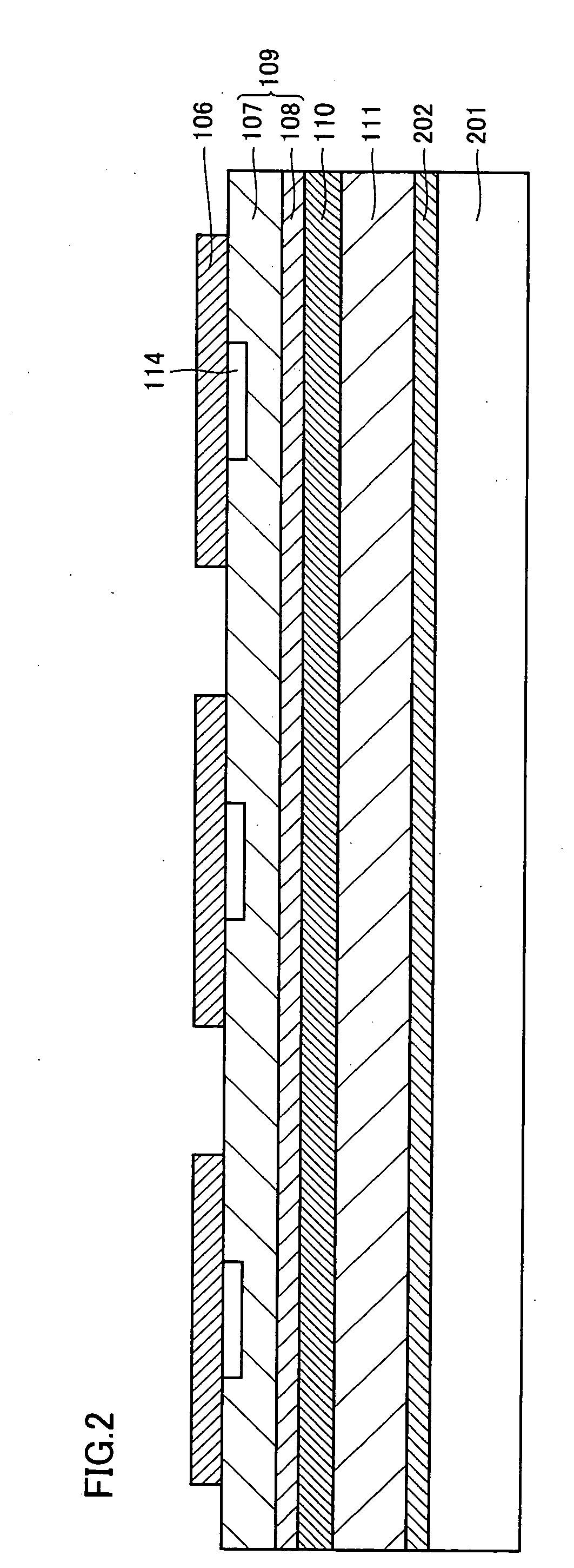
[0063]A nitride semiconductor light-emitting device having the structure shown in FIG. 1 was fabricated by the following method, as described with reference to FIGS. 2 to 7: First, a buffer layer 202 made of GaN; an n-type nitride semiconductor layer 111 consisting of an n-type GaN layer having a thickness of 4 μm; a light-emitting layer 110 (having a thickness of 100 nm) which is an MQW structure consisting of six periods of GaN barrier layer and InGaN well layer; and a p-type nitride semiconductor layer 109 consisting of a p-type AlGaN layer 108 (having a thickness of 20 nm) and a p-type GaN layer 107 (having thickness of 80 nm) were grown on a growth substrate 201 of sapphire in this order by MOCVD (step (A); see FIG. 2). Then, a photoresist mask having circular openings of 90 μm in diameter at a pitch of 400 μm was formed on the p-type GaN layer 107, in order to form current blocking regions 114. Then, portions of the p-type GaN layer 107 exposed in the openings of the photoresi...


PUM


Abstract

A nitride semiconductor light-emitting device including a reflecting layer made of a dielectric material, a transparent conductive layer, a p-type nitride semiconductor layer, a light emitting layer and an n-type nitride semiconductor layer in this order and a method of manufacturing the same are provided. The transparent conductive layer is preferably made of a conductive metal oxide or an n-type nitride semiconductor, and the reflecting layer made of a dielectric material preferably has a multilayer structure obtained by alternately stacking a layer made of a dielectric material having a high refractive index and a layer made of a dielectric material having a low refractive index.

Description

[0001]This nonprovisional application is based on Japanese Patent Application No. 2008-201971 filed on Aug. 5, 2008 with the Japan Patent Office, the entire contents of which are hereby incorporated by reference.BACKGROUND OF THE INVENTION[0002]1. Field of the Invention[0003]The present invention relates to a nitride semiconductor light-emitting device and a method of manufacturing the same.[0004]2. Description of the Background Art[0005]A nitride semiconductor light-emitting device having a one-side two-electrode structure obtained by stacking an n-type nitride semiconductor layer, a light emitting layer, a p-type nitride semiconductor layer and the like on an insulating sapphire substrate and arranging a p-side electrode and an n-side electrode on such a multilayer structure is known in general. In the nitride semiconductor light-emitting device having such a one-side two-electrode structure, however, the electrodes are not formed on symmetrical positions of the upper and lower su...

Claims


Application Information

Patent Timeline
IPC IPC(8): H01L33/00
CPCH01L33/0079H01L33/145H01L33/22H01L2933/0016H01L33/42H01L33/46H01L33/387H01L33/0093
Inventor FUDETA, MAYUKO
Owner XIAMEN SANAN OPTOELECTRONICS CO LTD
Learn More