System and method for reducing flicker noise from CMOS amplifiers

a technology of correlated low frequency noise and amplifier, which is applied in the direction of amplifiers with semiconductor devices only, amplifiers with semiconductor devices, amplifiers, etc., can solve the problems of objectionable artifacts in acquired images, noise in the bias circuit to be correlated, and each of these techniques has one or more limitations, so as to reduce correlated low frequency noise

Inactive Publication Date: 2010-01-21
GENERAL ELECTRIC CO
View PDF7 Cites 4 Cited by
  • Summary
  • Abstract
  • Description
  • Claims
  • Application Information

AI Technical Summary

Benefits of technology

[0007]Briefly, in accordance with one aspect of the technique, a data acquisition circuit is provided. The data acquisition circuit includes a plurality of data channels comprising a plurality of amplifiers and a biasing circuit for providing bias voltages to the plurality of amplifiers. The biasing circuit is configured to generate the bias voltages and establish a relationship between the bias voltages so as to reduce correlated low frequency noise in the plurality of amplifiers.
[0008]In accordance with another aspect of the technique, a data acquisition circuit is provided. The data acquisition circuit includes a plurality of data channels comprising a plurality of amplifiers and a biasing circuit for providing a first bias voltage and a second bias voltage to the plurality of amplifiers. The biasing circuit includes a master bias generator for generating the first bias voltage and a bias noise compensator coupled to the master bias generator for generating the second bias voltage proportional to the first bias voltage so as to reduce correlated low frequency noise in the plurality of amplifiers.

Problems solved by technology

However, this approach causes any noise in the bias circuit to be correlated across all the channels sharing the bias circuit.
This causes objectionable artifacts in the acquired images.
However each of these techniques has one or more limitations.
For example, BiCMOS or JFET amplifiers are expensive thereby making the detector circuit costly.
Alternatively, the use of differential amplifiers increases the power requirement and other noises.
Moreover, the use of separate bias circuits per channel increases the power and area requirement and is expensive.

Method used


Image

  • System and method for reducing flicker noise from CMOS amplifiers
  • System and method for reducing flicker noise from CMOS amplifiers
  • System and method for reducing flicker noise from CMOS amplifiers

Examples


Embodiment Construction

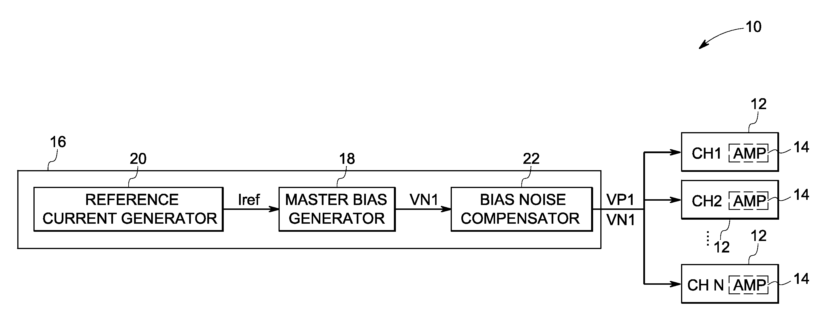
[0014]Embodiments of the present invention are generally directed to correlated low frequency noise reduction techniques in complementary metal oxide semiconductor (CMOS) amplifiers. Such embodiments may be used in a variety of semiconductor devices, such as for bipolar junction transistor (BJT) based devices, field effect transistor (FET) based devices, and so forth. Moreover, such embodiments may be used in a variety of applications, such as for data acquisitions, data reception and / or transmission, data conversion, data storage and so forth. Though the present discussion provides examples in a data acquisition context with respect to CMOS amplifiers, the application of these embodiments in other contexts and in other devices is well within the scope of the present invention.

[0015]Referring now to FIG. 1, a schematic of an exemplary data acquisition circuit 10 is illustrated in accordance with aspects of the present technique. The data acquisition circuit 10 includes multiple data...


PUM


Abstract

A technique is provided for acquiring data with reduced correlated low frequency noise interference via a data acquisition circuit. The data acquisition circuit includes a plurality of data channels comprising a plurality of amplifiers and a biasing circuit for providing bias voltages to the plurality of amplifiers. The biasing circuit is configured to generate the bias voltages and establish a relationship between the bias voltages so as to reduce correlated low frequency noise in the plurality of amplifiers.

Description

BACKGROUND[0001]The invention relates generally to noise reduction techniques, and more particularly to techniques for reducing correlated low frequency noise in a complementary metal oxide semiconductor (CMOS) amplifier.[0002]Data acquisition circuits are used in a wide range of applications requiring high quality data acquisition and processing. For example, in the field of medical imaging, imaging panels may detect the impinging radiation and convert them into measurable electrical charge through sensors. A data acquisition circuit may then read the electrical charge from the sensors in the imaging panel for subsequent conversion into digital data and image processing.[0003]The first stage of a data acquisition system is typically a low noise amplifier, whose main function is to provide enough gain to overcome the noise of subsequent stages and transform charges into voltage for further processing in some applications. Aside from providing this gain, a LNA should add as little no...

Claims


Application Information

Patent Timeline
Patent Type & Authority Applications(United States)
IPC IPC(8): H03F3/04
CPCH03F1/301
Inventor RAO, NARESH KESAVANCRONCE, RICHARD GORDONGUO, JIANJUN
Owner GENERAL ELECTRIC CO
Why Eureka
Try Eureka