Solar cell module
a solar cell and module technology, applied in the field of solar cell modules, can solve the problems of warping of the photovoltaic element by the stress generated inside the protection layer, and achieve the effects of reducing the stress at the projected portion, reducing warpage and peeling of the photovoltaic element, and improving weather resistan
- Summary
- Abstract
- Description
- Claims
- Application Information
AI Technical Summary
Benefits of technology
Problems solved by technology
Method used
Image
Examples
examples
[0054]Hereinafter, a thing solar cell module according to the present invention will be described specifically by way of Examples. The present invention, however, is not limited to the following Examples, and thus can be carried out by making appropriate changes without departing from the scope of the invention.
[0055](Method for Producing Solar Cell Module)
[0056]Hereinbelow, a method for producing a solar cell module according to Examples of the present invention will be described.
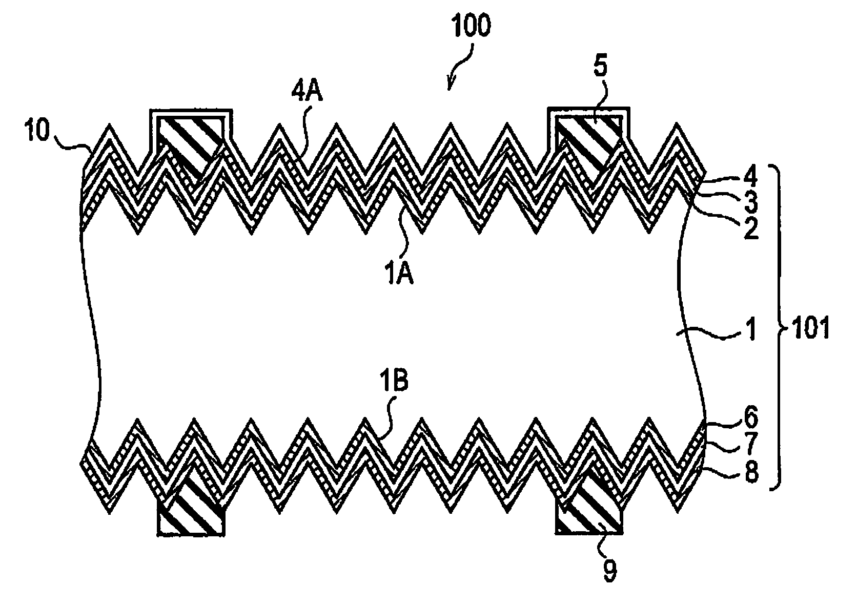
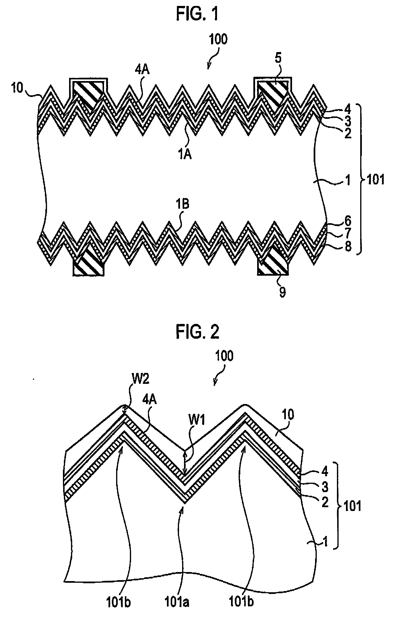
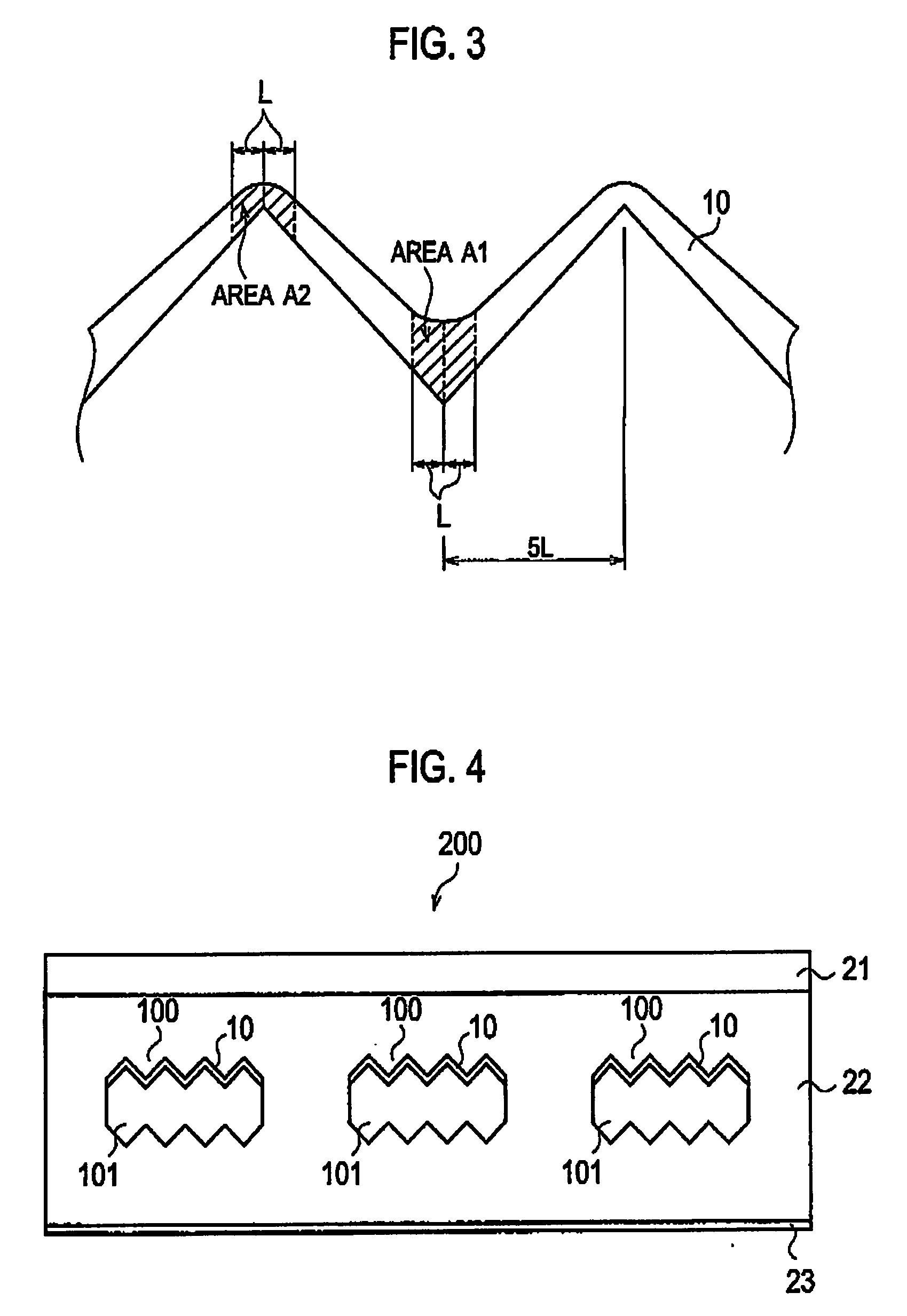
[0057]Anisotropic etching was conducted on the surface of an n type (100) single crystal silicon wafer having a specific resistance of approximately 1 Ω·m and a thickness of 800 μm, and a texture surface was formed. Then, the n type (100) single crystal silicon wafer was subjected to generally adapted cleaning to remove impurities. Subsequently, by using a known RF plasma CVD (13.56 MHz), at a forming temperature from 100 to 300° C., reaction pressure from 5 to 100 Pa, and RF power from 1 to 500 W / cm2, i t...
experiment 1
[0066]Protection layers including ZnO minute particles having a particle diameter of approximately 20 nm (ZnO content 75%) were formed on photoelectric conversion bodies by use of two types of sprays. Note that, here, the protection layers were formed only on the light entering sides. The material of the used protection layer had a low viscosity of approximately 1 cp. A spray A coats a target with the protection material in a form of shower at a high pressure, and thereby can form the protection layer in a manner that the protection layer is thick at a recessed portion and thin at a projected portion. A spray B coats a target with the protection material in a form of spiral, and thereby can form the protection layer with substantially uniform film thickness regardless of recessed and projected portions. Incidentally, the coating amount of protection material was adjusted, so that both sprays performed coating at approximately the same amount. The thicknesses of the protection layers...
experiment 2
[0075]From the result obtained in Experiment 1, it was found out that the film thickness structure at the projected portion should be thin. On the other hand, it was also found out that, in order to maintain the weather resistance of the overall element, the film thickness structure at the recessed portion is desirably thick. For this reason, the influence of the stress at the recessed portion on the weather resistance was checked. With the spray A, a target was coated with a single acrylic layer having a comparatively large stress. As a result, it was found out that the warped photovoltaic element was observed after the target was coated with the acrylic layer and dried. The reason is considered as follows. With the spray A, the recessed portion had a comparatively thick film structure. The warpage was shown to be largely relying on the influence of the stress at the recessed portion. Particularly, when the protection layer expands at the recessed portion, the large force is exerte...
PUM
 Abstract
Description
Claims
Application Information
 - R&D
- Intellectual Property
- Life Sciences
- Materials
- Tech Scout
- Unparalleled Data Quality
- Higher Quality Content
- 60% Fewer Hallucinations
Browse by: Latest US Patents, China's latest patents, Technical Efficacy Thesaurus, Application Domain, Technology Topic, Popular Technical Reports.
© 2025 PatSnap. All rights reserved.Legal|Privacy policy|Modern Slavery Act Transparency Statement|Sitemap|About US| Contact US: help@patsnap.com


