Radiation detector using gas amplication and method for manufacturing the same

Active Publication Date: 2009-12-31
DAI NIPPON PRINTING CO LTD
View PDF1 Cites 4 Cited by
  • Summary
  • Abstract
  • Description
  • Claims
  • Application Information

AI Technical Summary

Benefits of technology

[0021]As a result, if a large voltage is applied between the edges of the first electrode pattern and the convex portions of the second electrode pattern, that is, between the pixel electrode and the strip cathode electrode, the occurrence of arc discharge therebetween can be prevented. Therefore, the radiation detector can exhibit a high detection sensitivity due to the application of the large voltage therebetween.
[0024]According to the aspect of the present invention, therefore, the surface state of the pixel electrode (i.e., the protrusions thereof) can be shaped in a continuous curved surface by covering the convex portions of the second electrode pattern with a solder material so that the local electric concentration of the electric field for the pixel electrode can be prevented. As a result, the radiation detector can exhibit a high detection sensitivity due to the high voltage to be applied.
[0025]In the present invention, the wordings “continuous first curved surface” and “continuous second curved surface” mean that the surface state is smooth without local deformation such as protrusion and depressed portion from the starting point of the surface to the ending point thereof.
[0026]Moreover, since the edges of the first electrode pattern as the strip cathode electrode are shaped in curved surfaces respectively and / or the convex portions of the second electrode pattern as the pixel electrode are shaped in hemispherical surfaces respectively, the curved surfaces being curved outward from the corresponding edges of the first electrode pattern and the hemispherical surfaces being curved outward, the curvatures of the curved surfaces and the hemispherical surfaces become large, so that the electric concentration for the edges of the first electrode pattern and / or the convex portions of the second electrode pattern can be prevented, thereby suppressing the arc discharge at the edges thereof and / or the convex portions thereof effectively and efficiently. As a result, the radiation detector can absolutely exhibit a high detection sensitivity dependent on the amplitude of the voltage to be applied.
[0027]In the case where the surface state of the pixel electrode is nonuniform such that some protrusions and the like are formed on the surface of the pixel electrode, as described above, the electric concentration of the electric field on the protrusions and the like can be suppressed by covering the convex portions of the second electrode pattern as the pixel electrode with a solder material even though the edges of the first electrode pattern are not covered with a solder material, so that the arc discharge between the convex portions of the second electrode pattern as the pixel electrode and the edges of the first electrode pattern as the strip cathode electrode can be suppressed.

Problems solved by technology

In contrast, when the through holes are narrowed, the via-fill plating can not be uniformly carried out for the through holes so that the pixel electrode can not be also formed uniformly.
In this case, anomalous discharge and dielectric breakdown disadvantageously occur.
As a result, as of now, the voltage to be applied to the pixel electrode can not be sufficiently developed while the narrowing of the pixel electrode can not be sufficiently realized, so that the detection sensitivity of the pixel radiation detector can not be sufficiently enhanced.

Method used


Image

  • Radiation detector using gas amplication and method for manufacturing the same
  • Radiation detector using gas amplication and method for manufacturing the same
  • Radiation detector using gas amplication and method for manufacturing the same

Examples


Embodiment Construction

[0039]Hereinafter, the present invention will be described in detail with reference to the drawings.

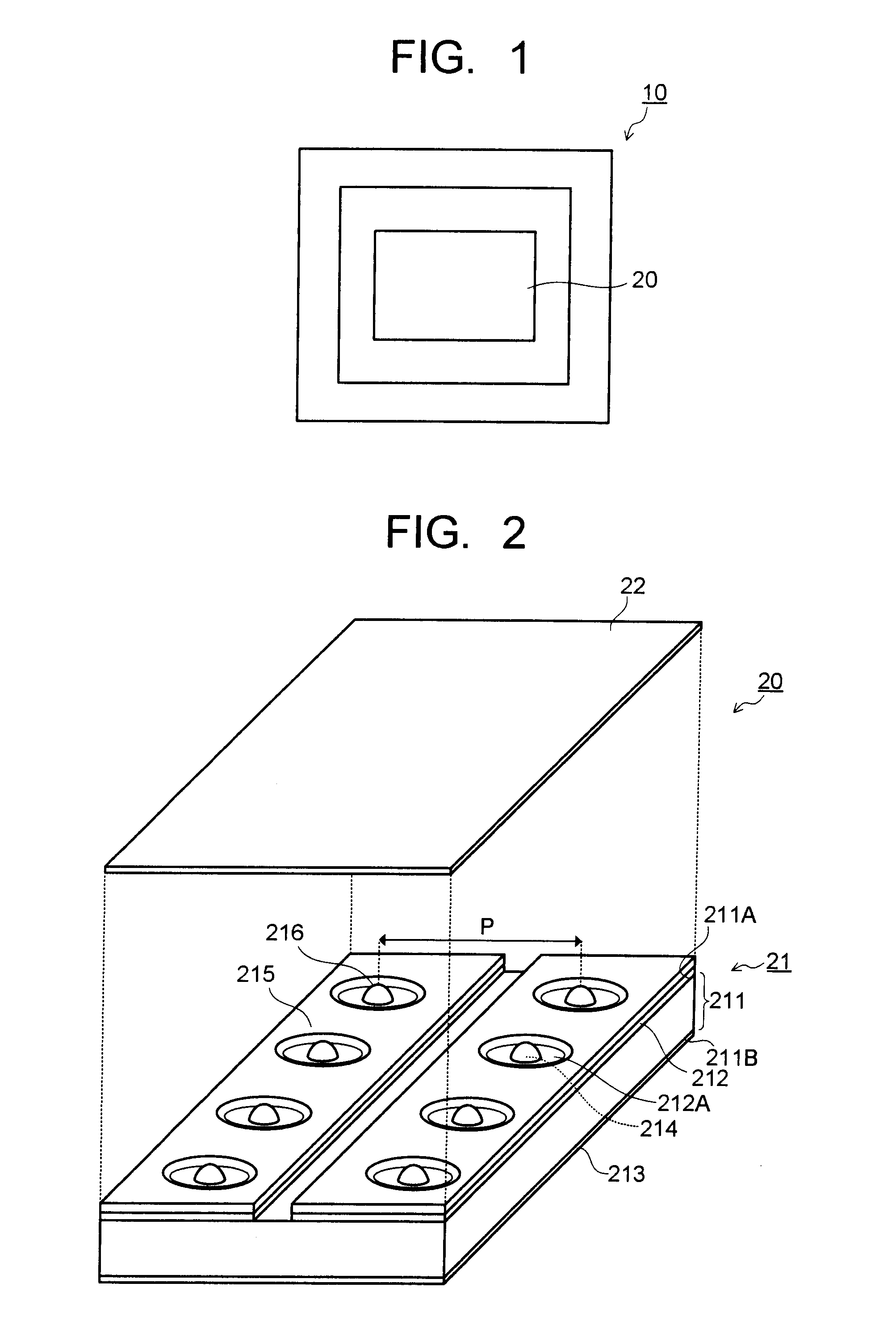
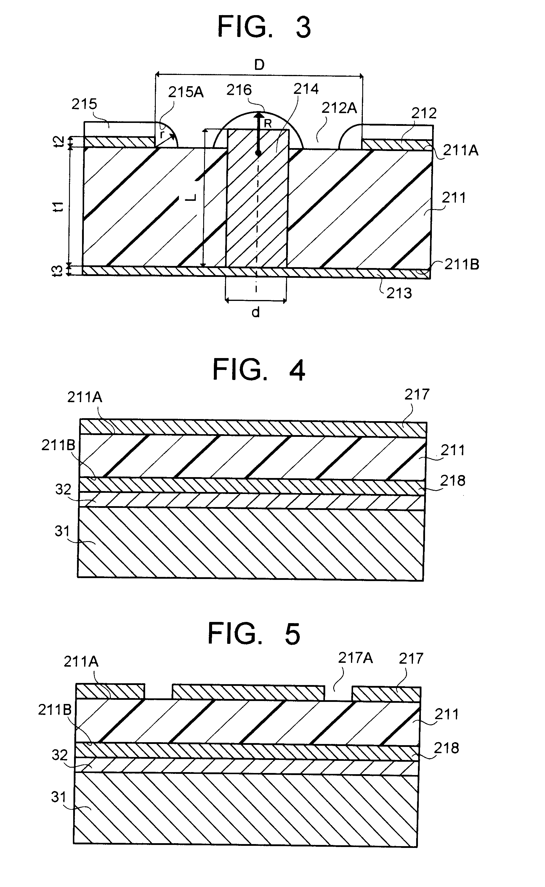
[0040]FIG. 1 is a plan view schematically showing the structure of the radiation detector according to an embodiment of the present invention. FIG. 2 is a perspective view enlargedly showing the pixel radiation detector of the radiation detector shown in FIG. 1. FIG. 3 is a cross sectional view enlargedly showing the area around the pixel electrode of the pixel radiation detector.

[0041]As shown in FIG. 1, a radiation detector 10 in this embodiment includes a pixel radiation detector 20 and a current detecting circuit (not shown). As shown in FIG. 2, the pixel radiation detector 20 includes a detecting panel 21 and an electrode plate 22 which is provided above the detecting panel 21 so as to be opposite thereto.

[0042]As shown in FIG. 2, the detecting panel 21 includes a first electrode pattern 212 with a plurality of circular openings 212A which is formed on the main surface 211A of an...


PUM

PropertyMeasurementUnit
Electric potential / voltageaaaaaaaaaa

Abstract

A radiation detector using gas amplification includes: a first electrode pattern which is formed on a first surface of an insulating member and has a plurality of circular openings; and a second electrode pattern which is formed on a second surface of the insulating member opposite to the first surface thereof and has convex portions of which respective forefronts are exposed to centers of the openings of the first electrode pattern; wherein a predetermined electric potential is set between the first electrode pattern and the second electrode pattern; wherein edges of the first electrode pattern exposing to the openings are shaped in respective continuous first curved surfaces by covering the edges thereof with a first solder material.

Description

CROSS-REFERENCE TO RELATED APPLICATIONS[0001]This application is based upon and claims the benefit of priorities from the prior Japanese Patent Application No. 2008-163205 filed on Jun. 23, 2008 and Japanese Patent Application No. 2009-138019 filed on Jun. 9, 2009; the entire contents which are incorporated herein by reference.BACKGROUND[0002]1. Field of the Invention[0003]The present invention relates to a radiation detector with a pixel electrode using gas amplification and a method for manufacturing the radiation detector.[0004]2. Background of the Invention[0005]Conventionally, a pixel radiation detector would be employed as a radiation detector using gas amplification. In the conventional pixel radiation detector, a strip cathode electrode is formed on the main surface of a double-sided printed substrate and a strip anode electrode is formed on the rear surface of the same printed substrate while openings are formed in the strip cathode electrode at a constant pitch and columna...

Claims


Application Information

Patent Timeline
IPC IPC(8): G01T1/00G03F7/20
CPCY10T29/49156G01T1/185
Inventor MOTOMURA, TOMOHISASHIMADA, OASMU
Owner DAI NIPPON PRINTING CO LTD
Why Eureka
Try Eureka