
Neuralprobe and methods for manufacturing same

Inactive Publication Date: 2009-12-24
UNIV OF FLORIDA RES FOUNDATION INC
View PDF5 Cites 34 Cited by
  • Summary
  • Abstract
  • Description
  • Claims
  • Application Information

AI Technical Summary

Benefits of technology

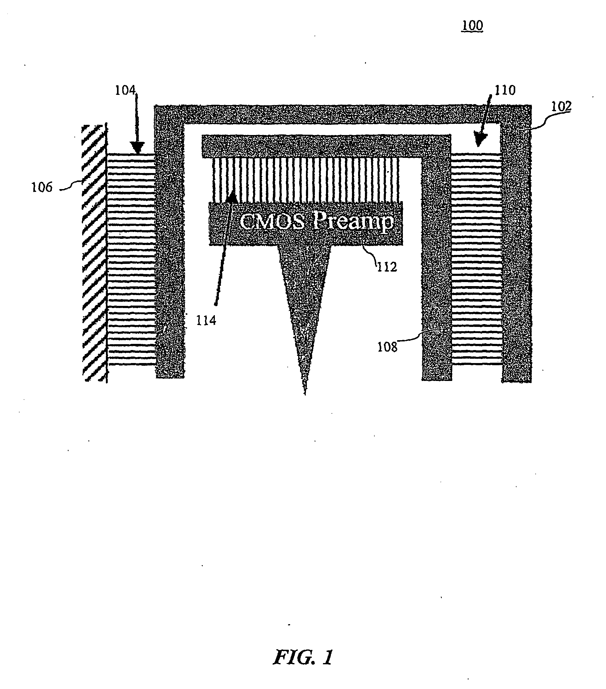
[0007]The present invention provides a neural probe and related methods for manufacturing such a probe. More particularly, one aspect of the invention is a probe that operates according to three modes. The first mode is a large-signal motion mode of operation for “tuning in” single-unit neuronal activity. The second mode is a small-signal motion mode of operation with lock-in amplifier that increases a signal-to-noise ration (SNR). The third mode is a burst small-signal motion mode of operation for clearing tissue responses. By being capable of operating according to these modes, the probe can provide enhanced sensing and recording of neuronal activity.
[0010]Another aspect of the invention is a method of manufacturing a neural probe from a processed CMOS chip. Post-CMOS processing according to the invention can incorporate self-aligned selective nickel plating and sacrifices two aluminum layers. The fabrication technique can produce a neural probe in which the sensing elements are in close proximity to CMOS circuitry. The fabrication technique, moreover, can eliminate the need for post-CMOS masks, alignment, or assembly.

Problems solved by technology

One yet-to-be-resolved obstacle confronting designers of conventional subdural microelectrode neural prosthetics is the limited control of probe-to-neuron distance owing to the fixed probe length of many conventional devices.
Another obstacle is the low signal level that is to be sensed with such a device, the level typically being on the order of only several microvolts.
Still another obstacle is the gradual decline in sensitivity of the neural probe that often occurs over time.
These and other approaches, however, have typically failed to adequately address the problems already described concerning conventional devices.

Method used


Image

  • Neuralprobe and methods for manufacturing same
  • Neuralprobe and methods for manufacturing same
  • Neuralprobe and methods for manufacturing same

Examples


Embodiment Construction

[0021]The invention provides a neural probe and related methods for fabricating a neural probe. The neural probe, more particularly, can comprise a micro-machined moveable neural probe that operates according to three distinct modes of operation. The first mode pertains to large-signal motion for “tuning in” to single-unit neuronal activity. The second mode pertains to small-signal motion with an amplifier lock-in to increase signal-to-noise ratios. The third mode of operation pertains to burst small-signal motion for clearing tissue responses.

[0022]Through these distinct modes of operation, a neural probe according to the invention can overcome limitations inherent in conventional devices such as the limited control of probe-to-neuron distance due to the fixed probe length of various types of conventional devices. The neural probe according to the invention can also overcome limitations occurring as a result of the low level—typically only a few microvolts—of signals that are sense...


PUM


Abstract

A neural probe and method of fabricating same are provided. The probe comprises a plurality of frames connected to each other and to a substrate by respective bimorphs. A probe base is connected by another bimorph to the frames. A probe tip extends from the probe base. The probe can achieve a large vertical motion and out-of-plane curling. The probe can operate according to three modes. The first mode pertains to a large-signal motion for tuning in single-unit neuronal activity. The second pertains to a small-signal motion with lock-in amplifier that increases SNR. The third pertains to burst small-signal motion for clearing tissue responses. Fabrication of a neural probe begins with a processed CMOS chip. Post-CMOS processing incorporates self-aligned selective nickel plating and sacrifices two aluminum layers. The fabrication technique produces a neural probe in which the sensing elements are in close proximity to CMOS circuitry. The fabrication technique obviates the need for post-CMOS masks, alignment, or assembly.

Description

FIELD OF THE INVENTION[0001]The present invention is related to the field of electronic sensors, and more particularly, to electronic sensors for sensing neuronal activity.BACKGROUND OF THE INVENTION[0002]Neural prosthetics are chips that model brain function and that can be implanted in a living organism to replace damaged or dysfunctional portions of the brain or other tissue of the organism's nervous system. For example, a neural prosthetic can comprise an intracranial implant or computer chip that models a brain function so as to replace damaged or dysfunctional brain tissue. As a result of relatively recent advances in neuroscience and bioengineering, there is a likelihood of more biologically realistic mathematical models of the brain and spinal cord functions, as well as silicon and / or photonics-based computational devices that can incorporate such models. In addition, there is a drive for enhanced neuron-silicon interface devices, such as micro-scale electrodes that can prov...

Claims


Application Information

Patent Timeline
IPC IPC(8): A61B5/0478H01L21/465
CPCA61B2562/028A61B5/04001A61B5/24A61B5/294
Inventor NISHIDA, TOSHIKAZUXIE, HUIKAIPATRICK, ERIN E.SANCHEZ, JUSTIN C.
Owner UNIV OF FLORIDA RES FOUNDATION INC
Learn More