Embedded thin films
a technology of embedded thin films and thin films, which is applied in the direction of printed resistor incorporation, coating, printed capacitor incorporation, etc., can solve the problems of energy inefficiency, metal embrittlement and/or separation of conductors from substrates, and suboptimal properties of resulting devices, so as to reduce the hydrolysis generation of hydrogen and avoid corrosive conditions
- Summary
- Abstract
- Description
- Claims
- Application Information
AI Technical Summary
Benefits of technology
Problems solved by technology
Method used
Image

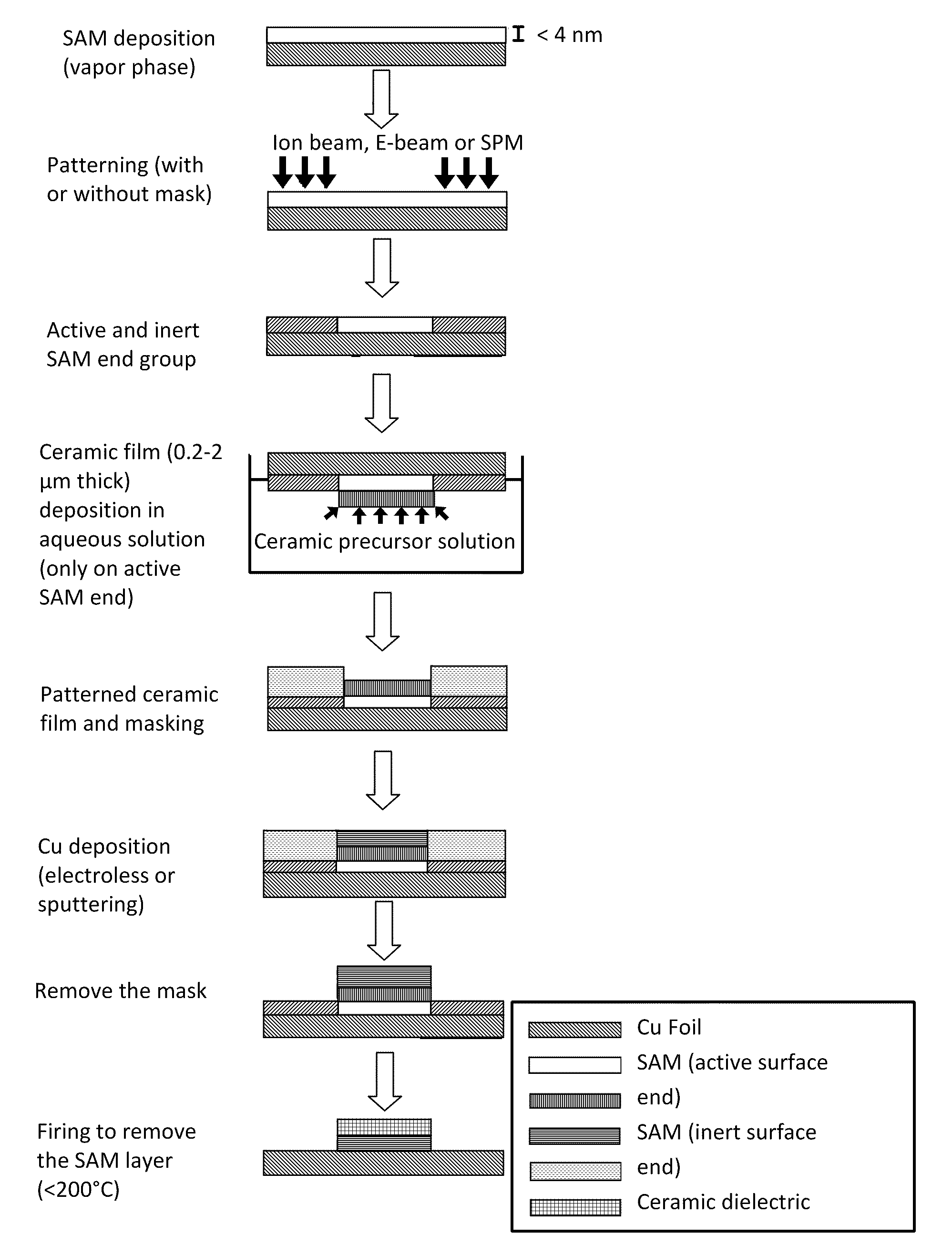
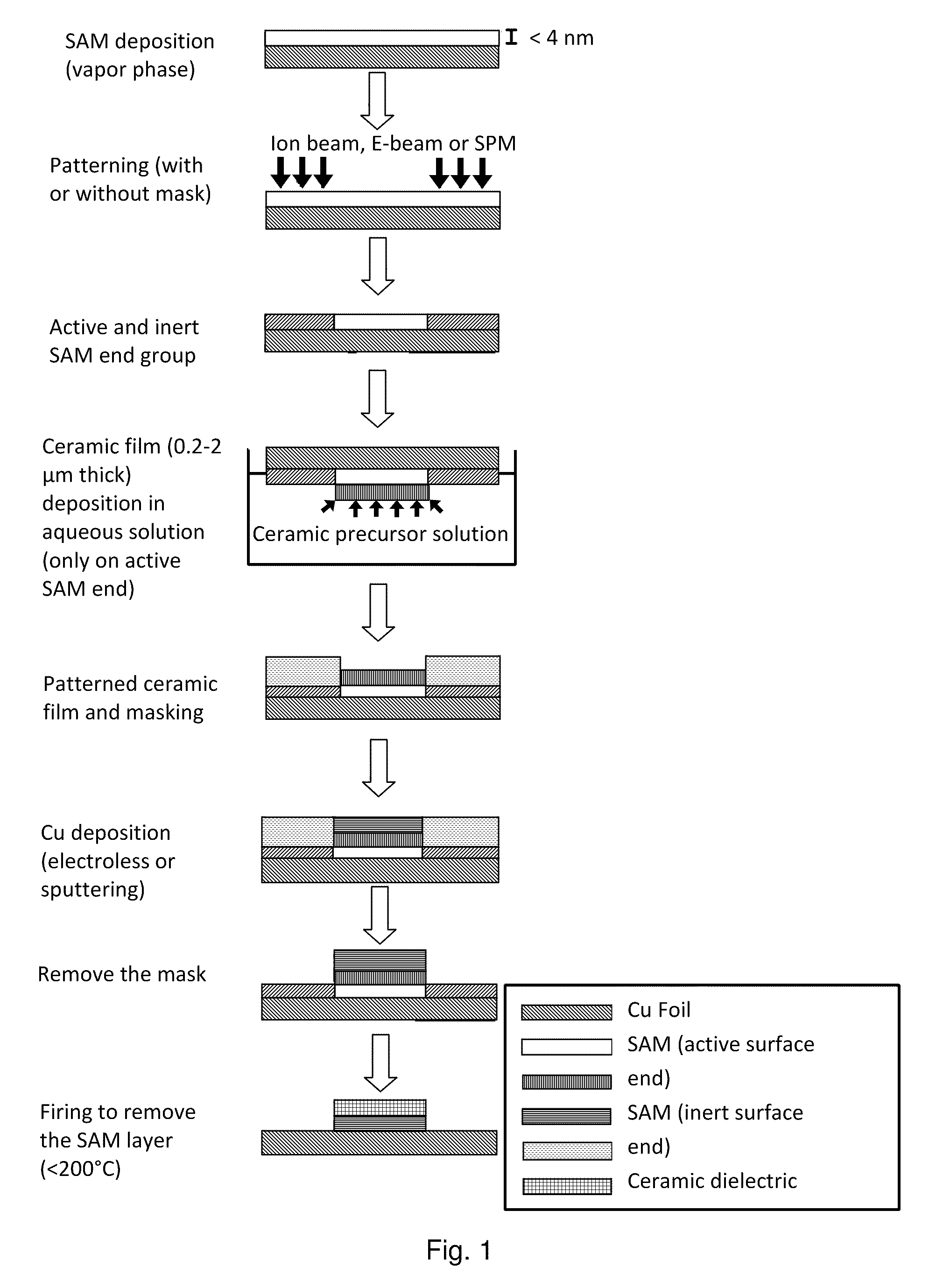
Examples
example 2
[0078]A ceramic film was deposited under the following conditions:
[0079]Solution: Methanol:Water=1:1 v / v, TiCl4=0.02 M, H2O2=0.2
[0080]Voltage: 10V, Electrode distance 2 cm, CD=100 mA / cm2, Time 120 s
[0081]The process produced a 2000-nm thick film, which is shown in the photomicrographs of FIGS. 4A, 4B, and 4C at varying increasing magnifications.
example 3
[0082]A deposition of titania films on commercial copper / FR4 / copper laminates was conducted under the following conditions:
[0083]Solution: Methanol:Water=95:5 v / v, TiCl4=0.02 M, H2O2=0.1 M
[0084]Voltage: 10V, Electrode distance 2 cm, CD=100 mA / cm2, Time 20 / 20 / 20 s (three 20 second intervals). Multiple deposition periods were adopted to reduce through-the-layer cracks. Electron micrographs of the resultant films are shown in FIGS. 5A and 5B, at varying magnification.
example 4
[0085]A deposition was conducted of titania films on 500 nm thick copper sputtered on a polyimide (PI) surface under the following conditions:
[0086]Solution: Methanol:Water=95:5 v / v, TiCl4=0.02 M. (without H2O2 in the electrolyte.)
[0087]Voltage: 10V, Electrode distance 2 cm, CD=15 mA / cm2, Time 120 s
[0088]The process, which did not use hydrogen peroxide, produces a very porous structure, with evident cracking at lower magnifications, as shown in FIGS. 6A, 6B and 6C.
PUM
| Property | Measurement | Unit |
|---|---|---|
| thickness | aaaaa | aaaaa |
| temperature | aaaaa | aaaaa |
| voltage potential | aaaaa | aaaaa |
Abstract
Description
Claims
Application Information
 - R&D
- Intellectual Property
- Life Sciences
- Materials
- Tech Scout
- Unparalleled Data Quality
- Higher Quality Content
- 60% Fewer Hallucinations
Browse by: Latest US Patents, China's latest patents, Technical Efficacy Thesaurus, Application Domain, Technology Topic, Popular Technical Reports.
© 2025 PatSnap. All rights reserved.Legal|Privacy policy|Modern Slavery Act Transparency Statement|Sitemap|About US| Contact US: help@patsnap.com