Method for making low Vt gate-first light-reflective-layer covered dual metal-gates on high-k CMOSFETs

a technology of dielectric cmosfets and metal gates, which is applied in the direction of basic electric elements, electrical apparatus, and semiconductor devices, can solve the problems that the spd formed usj is not compatible with the current vlsi fabrication process, and achieve low vt in metal gates/high- cmosfets, simple process of ion implantation, and high mobility

Inactive Publication Date: 2009-10-22
CHIN ALBERT
View PDF18 Cites 3 Cited by
  • Summary
  • Abstract
  • Description
  • Claims
  • Application Information

AI Technical Summary

Benefits of technology

[0006]To overcome the drawbacks of the prior arts, this invention proposes a method with simpler processes of ion implantation, light-irradiation anneal and light-reflective gate to achieve low Vt in metal-gate/high-κ CMOSFETs. At 1.05 nm EOT, the self-aligned and gate-first p- and n-MOSFETs of this invention showed proper effective work-function (φm-eff) of 5.04 and 4.24 eV, low Vt of −0.16 and 0.13 V, high mobility of 85 and 209 cm2/Vs and good 85° C. bias-temperature-instability (BTI) reliability. Using this novel very high-κ value TiLaO gate dielectric, desired low Vt of −0.07 and 0.12 V and high mobility of 82 and 203 cm2/Vs were achieved for respective p- and n-MOSFETs even at small EOT of 0.63 nm. This was realized using light-irradiation annealing on ion-implanted source-drain area and light-reflective Al-covered gate electrode. In this invention, Al reflects as high as 91% of the KrF excimer (248 nm wa

Problems solved by technology

However, this SPD formed USJ is not compat

Method used


Image

  • Method for making low Vt gate-first light-reflective-layer covered dual metal-gates on high-k CMOSFETs
  • Method for making low Vt gate-first light-reflective-layer covered dual metal-gates on high-k CMOSFETs
  • Method for making low Vt gate-first light-reflective-layer covered dual metal-gates on high-k CMOSFETs

Examples


Embodiment Construction

[0020]For the best understanding of this invention, please refer to the following detailed description of the preferred embodiments and the accompanying drawings, wherein:

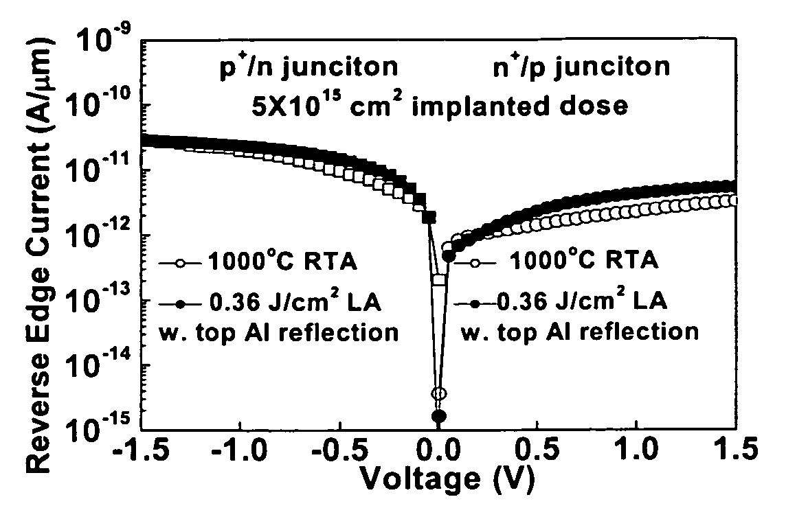
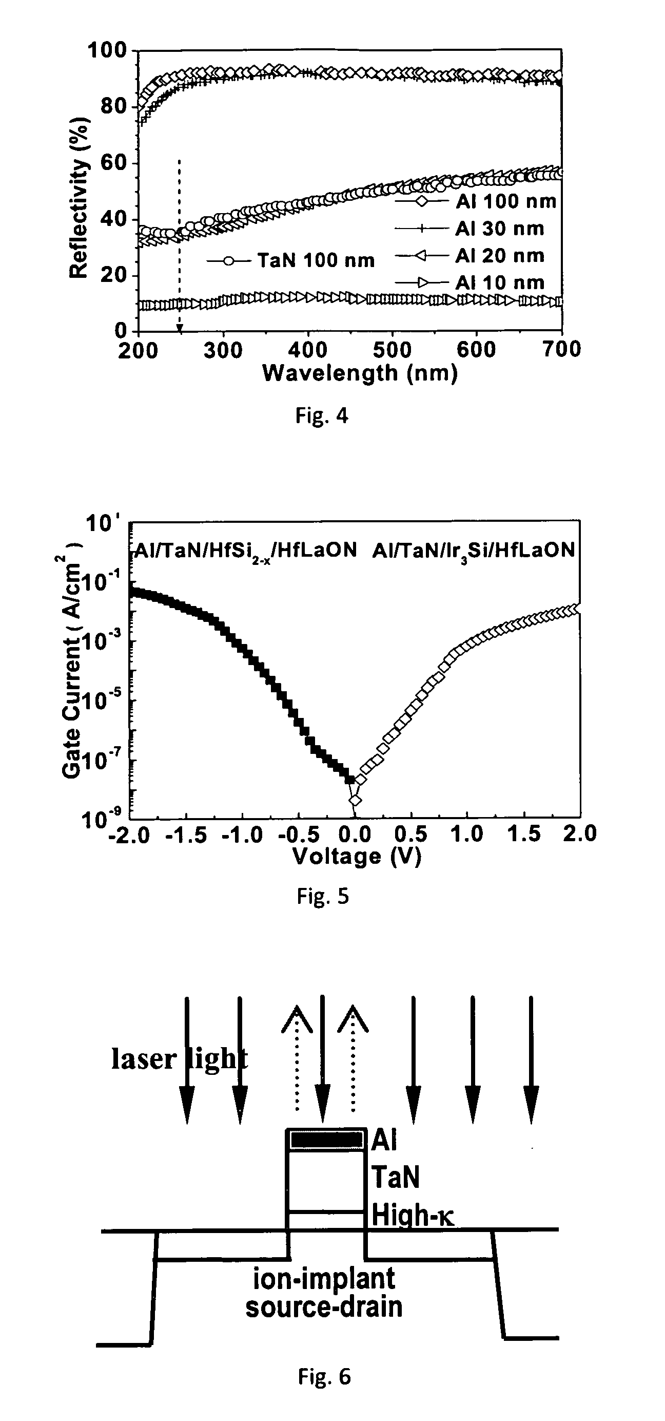
[0021]In view of the drawbacks of the prior arts, this invention proposes a method for making low Vt Gate-First light-reflective-layer / dual-metal-gates / high-κ CMOSFETs which added a thin light-reflection layer on top of dual metal-gates. FIG. 4 shows the optical reflectivity (R) vs. light wavelength. The R increases with Al layer thickness and reaches high R of 87% and 91% at 30 and 100 nm, even at short 248 nm KrF laser. It is important to notice that high R>90% is measured at longer UV wavelength to visible light wavelength. Therefore, this light-reflective method can also be used in Flash-light anneal method with additional UV-light filter. Using top Al laser-reflective gate, proper φm-eff of 5.04 and 4.24 eV are obtained with much improved VFB roll-off compared with conventional top TaN gate (FIGS. 2-3). Owing ...


PUM


Abstract

This invention proposes a method for making low Vt light-reflective-layer/dual-metal-gates/high-κ CMOSFETs with simple light-irradiation anneal and light-reflective-layer covered dual metal-gates with self-aligned and gate-first process compatible with current VLSI process. At 1.05 nm EOT, good φm-eff of 5.04 and 4.24 eV, low Vt of −0.16 and 0.13 V, high mobility of 85 and 209 cm2/Vs, and small 85° C. BTI≦40 mV (10 MV/cm, 1 hr) were measured for p- and n-MOSFETs. Using novel very high-κ TiLaO gate dielectric, low Vt of −0.07 and 0.12 V and high mobility of 82 and 203 cm2/Vs were achieved even at small EOT of 0.63 nm.

Description

BACKGROUND OF THE INVENTION [0001]1. Field of the Invention[0002]The invention relates to a method for making low threshold voltage (Vt) Gate-First Light-Reflective-Layer Covered Dual Metal-Gates on High-κ dielectric CMOSFETs Using Light-irradiation anneal. More particularly, the invention relates to a method for making low Vt Gate-First Dual Metal-Gates / High-κ CMOSFETs with laser or ultra-violate (UV) filtered Flash-light anneal.[0003]2. Description of the Related Art[0004]The toughest challenge for making metal-gate / high-κ CMOSFETs is to lower the undesired high Vt [1]*-[5]* (please refer to table 1 for detail prior arts [1]*-[6]*). Various high-κ dielectrics of Dy2O3 / HfO2, HfSiON, HfSi(Al)ON, HfLaON, and HfLaO with various dual metal gates for p / n MOSFETs of TaCxN / TaCx, Ni31Si12NiSi, TiAlN / TaSiN, Ni3Si / NiSi2, and Ir3Si / TaN were used, but the Vt values are still high or can only demonstrated at larger equivalent-oxide thickness (EOT). This is especially hard for p-MOSFET, since on...

Claims


Application Information

Patent Timeline
IPC IPC(8): H01L21/8238
CPCH01L21/26513H01L21/266H01L29/517H01L21/823842H01L29/4966H01L21/268
Inventor CHIN, ALBERT
Owner CHIN ALBERT
Why Eureka
Try Eureka