
Lateral diffusion field effect transistor with drain region self-aligned to gate electrode

a field effect transistor and drain region technology, applied in the field of lateral diffusion metaloxidesemiconductor field effect transistors, can solve the problems of reducing on-resistance, high resistance of the drift region b>140/b>, and undesirable, and achieve the effect of constant drift distan

Inactive Publication Date: 2009-10-22
GLOBALFOUNDRIES INC
View PDF33 Cites 33 Cited by
  • Summary
  • Abstract
  • Description
  • Claims
  • Application Information

AI Technical Summary

Benefits of technology

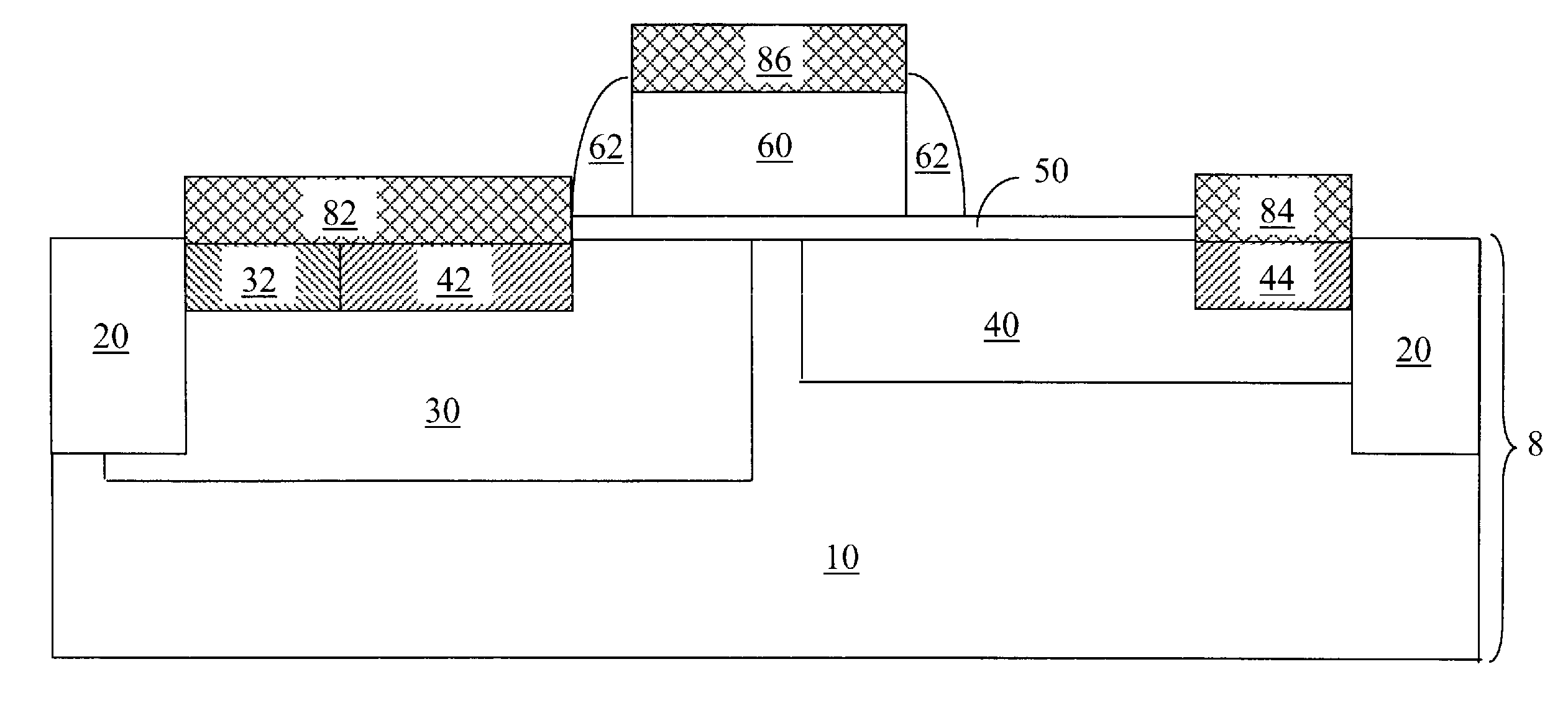
[0018]In the present invention, a disposable structure displaced from an edge of a gate electrode and a drain region aligned to the disposable structure is formed. Thus, the drain region is self-aligned to the edge of the gate electrode. In one embodiment, the disposable structure is a disposable spacer. In another embodiment, the disposable structure is formed simultaneously with, and comprises the same material as, a gate electrode. After formation of the drain regions, the disposable structure is removed. The self-alignment of the drain region to the edge of the gate electrode provides a substantially constant drift distance that is independent of any overlay variation of lithographic processes.

Problems solved by technology

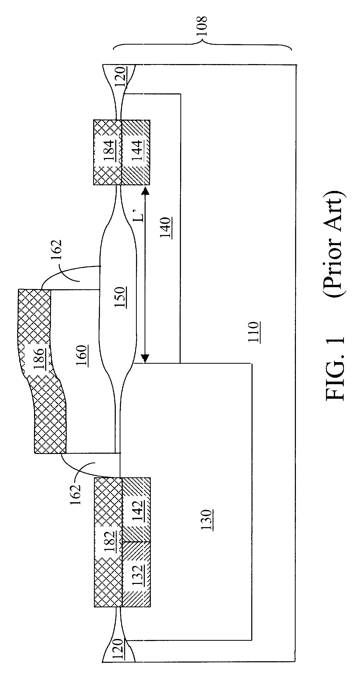
However, a high resistance of the drift region 140 is undesirable because current flow through the drift region 140 is impeded by such a high resistance.
However, the high resistance is undesirable in an on-state since the performance and efficiency is limited by the high resistance of the drift region.
Reduction of on-resistance of the drift region generally comes at the expense of decreased breakdown voltage and device reliability, thus limiting the allowable operating voltage.
Increase of resistance of the drift region results in an increase in the operating voltage at the expense of reduced performance and efficiency.

Method used


Image

  • Lateral diffusion field effect transistor with drain region self-aligned to gate electrode
  • Lateral diffusion field effect transistor with drain region self-aligned to gate electrode
  • Lateral diffusion field effect transistor with drain region self-aligned to gate electrode

Examples


Embodiment Construction

[0083]As stated above, the present invention relates to lateral diffusion metal-oxide-semiconductor field effect transistors (LDMOSFETs) having a drain region that is self-aligned to a gate electrode to provide a constant drift distance, and consequently, a constant drift region resistance, and methods of manufacturing the same, which are now described in detail with accompanying figures. It is noted that like and corresponding elements are referred to by like reference numerals.

[0084]Referring to FIG. 3, a first exemplary structure according to a first embodiment of the present invention comprises a semiconductor substrate 8 containing a substrate semiconductor region 10 and shallow trench isolation regions 20. The substrate semiconductor region 10 comprises a semiconductor material. For example, the substrate semiconductor region may comprise a first silicon containing material such as silicon, a silicon germanium alloy, a silicon carbon alloy, or a silicon germanium carbon alloy....


PUM


Abstract

A disposable structure displaced from an edge of a gate electrode and a drain region aligned to the disposable structure is formed. Thus, the drain region is self-aligned to the edge of the gate electrode. The disposable structure may be a disposable spacer, or alternately, the disposable structure may be formed simultaneously with, and comprise the same material as, a gate electrode. After formation of the drain regions, the disposable structure is removed. The self-alignment of the drain region to the edge of the gate electrode provides a substantially constant drift distance that is independent of any overlay variation of lithographic processes.

Description

FIELD OF THE INVENTION[0001]The present invention relates to semiconductor structures, and particularly to lateral diffusion metal-oxide-semiconductor field effect transistors (LDMOSFETs) having a drain region that is self-aligned to a gate electrode to provide a constant drift distance, and consequently, a constant drift region resistance, and methods of manufacturing the same.BACKGROUND OF THE INVENTION[0002]A lateral diffusion metal-oxide-semiconductor field effect transistor (LDMOSFET) is a field effect transistor having a drift region between a gate and a drain region in order to avoid a high electric field at a drain junction, i.e., at the p-n junction between a body and the drain region. An LDMOSFET is typically employed in high voltage power applications involving voltages in the range from about 5 V to about 50 V, which is applied across the drain region and the source region. A substantial fraction of the high voltage may be consumed within the drift region in the LDMOSFET...

Claims


Application Information

Patent Timeline
Patent Type & Authority Applications(United States)
IPC IPC(8): H01L29/78H01L21/336
CPCH01L21/26513H01L21/26586H01L29/7835H01L29/6656H01L29/66659H01L29/1045H01L29/665
Inventor FEILCHENFELD, NATALIE B.GAMBINO, JEFFREY P.LIU, XUEFENGVOEGELI, BENJAMIN T.VOLDMAN, STEVEN H.ZIERAK, MICHAEL J.
Owner GLOBALFOUNDRIES INC
Learn More