Semiconductor Device, Electronic Device, and Method of Manufacturing Semiconductor Device
a semiconductor and electronic technology, applied in the direction of solid-state devices, basic electric elements, thermoelectric devices, etc., can solve the problems of inevitable increase in manufacturing costs, and achieve the effects of stable formation, reduced material loss and cost, and high performan
- Summary
- Abstract
- Description
- Claims
- Application Information
AI Technical Summary
Benefits of technology
Problems solved by technology
Method used
Image
Examples
embodiment mode 1
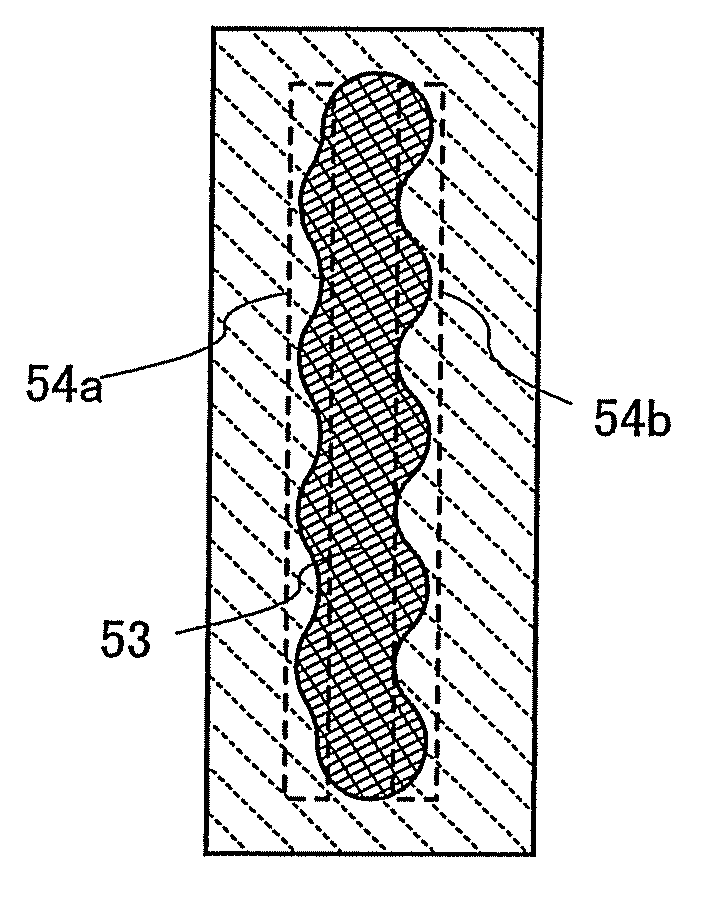
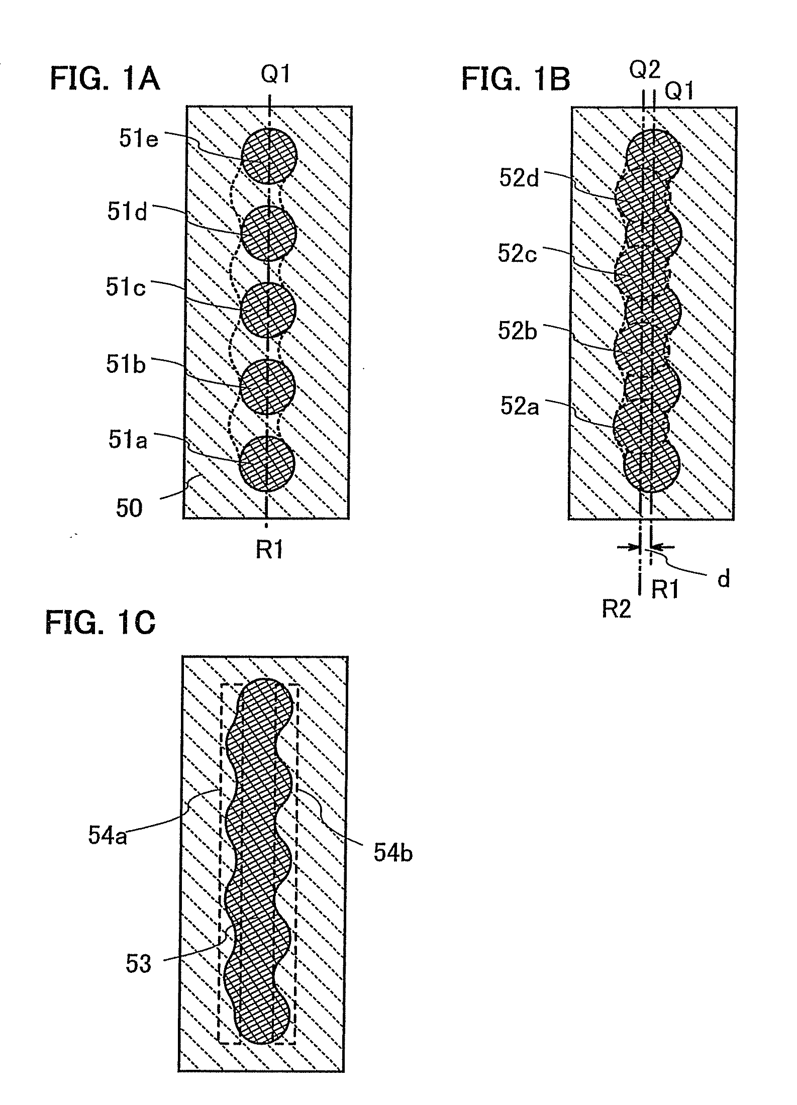
[0043]Embodiment Mode 1 of the present invention will be described with reference to FIGS. 1A to 1C.
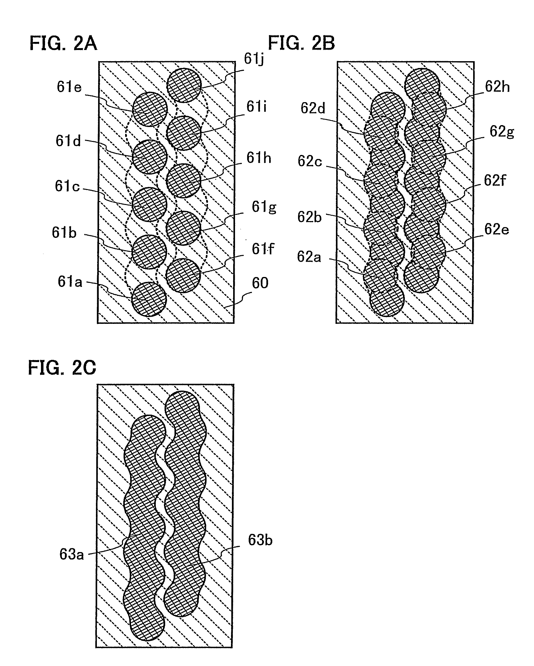
[0044]One feature of the present invention is that at least one or more of components required to manufacture a semiconductor device or a display device, such as a conductive layer for forming a wiring layer or an electrode, or a mask layer for forming a predetermined pattern, is / are formed by a method capable of selectively forming a component into a desired shape to manufacture a semiconductor device or a display device. In the present invention, a component (also referred to as a pattern) refers to a conductive layer such as a wiring layer, a gate electrode layer, a source electrode layer, or a drain electrode layer; a semiconductor layer; a mask layer; an insulating layer; or the like, which is included in a thin film transistor or a display device, and includes any component that is formed to have a predetermined shape. A droplet discharge (ejection) method (including an ink-jet ...
embodiment mode 2
[0080]In this embodiment mode, an example of a display device using the present invention will be described
[0081]FIG. 6A is a top view showing a structure of a display panel using the present invention. A pixel area 2701 in which pixels 2702 are arranged in matrix, a scan line input terminal 2703, and a signal line input terminal 2704 are formed over a substrate 2700 having an insulating surface. The number of the pixels may be determined in accordance with various standards. In the case of XGA and RGB display, the number of the pixels may be 1024×768×3 (RGB). Similarly, in the case of UXGA and RGB display, the number of the pixels may be 1600×1200×3 (RGB), and in the case of a full-spec high vision and RGB display, it may be 1920×1080×3 (RGB).
[0082]The pixels 2702 are formed in matrix at intersections of scan lines extended from the scan line input terminal 2703 and signal lines extended from the signal line input terminal 2704. Each pixel 2702 is provided with a switching element ...
embodiment mode 3
[0143]An embodiment mode of the present invention will be described using FIG. 3 and FIGS. 13A and 13B. Specifically, a method for manufacturing a display device to which the present invention is applied will be described. FIG. 3 is a top view of a pixel area of a display device. FIG. 13B is a cross-sectional view taken along line E-F of FIG. 3. FIG. 13A is also a top view of a display device. FIG. 13B is a cross-sectional view taken along line O-P (including line U-W) of FIG. 13A. Further, in this embodiment mode, an example of a liquid crystal display device in which a liquid crystal material is used for a display element is shown. Therefore, the same portions or portions having the same functions will not be repeatedly explained.
[0144]As a substrate 200, a glass substrate such as a barium borosilicate glass substrate, an alumino borosilicate glass substrate, a quartz substrate, a metal substrate, or a heat-resistant plastic substrate that can withstand a processing temperature of...
PUM
 Abstract
Description
Claims
Application Information
 - R&D
- Intellectual Property
- Life Sciences
- Materials
- Tech Scout
- Unparalleled Data Quality
- Higher Quality Content
- 60% Fewer Hallucinations
Browse by: Latest US Patents, China's latest patents, Technical Efficacy Thesaurus, Application Domain, Technology Topic, Popular Technical Reports.
© 2025 PatSnap. All rights reserved.Legal|Privacy policy|Modern Slavery Act Transparency Statement|Sitemap|About US| Contact US: help@patsnap.com


