Track and hold circuit
a track and hold circuit technology, applied in the field of track hold circuits, can solve the problems of reducing the overall signal-to-noise-and-distortion ratio (sndr), affecting the signal quality of the circuit, so as to improve the signal-to-noise-and-distortion-ratio (sndr)
- Summary
- Abstract
- Description
- Claims
- Application Information
AI Technical Summary
Benefits of technology
Problems solved by technology
Method used
Image
Examples
Embodiment Construction
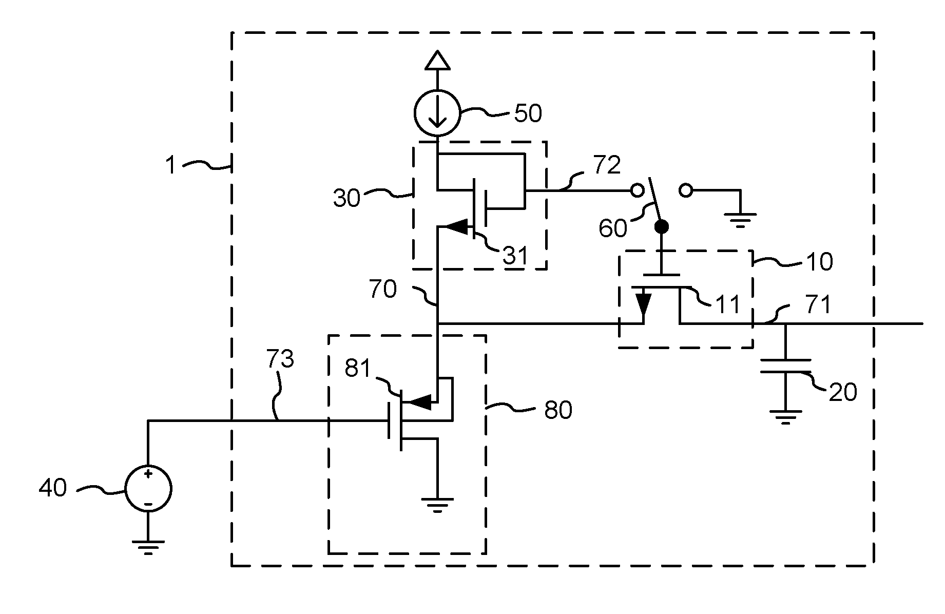
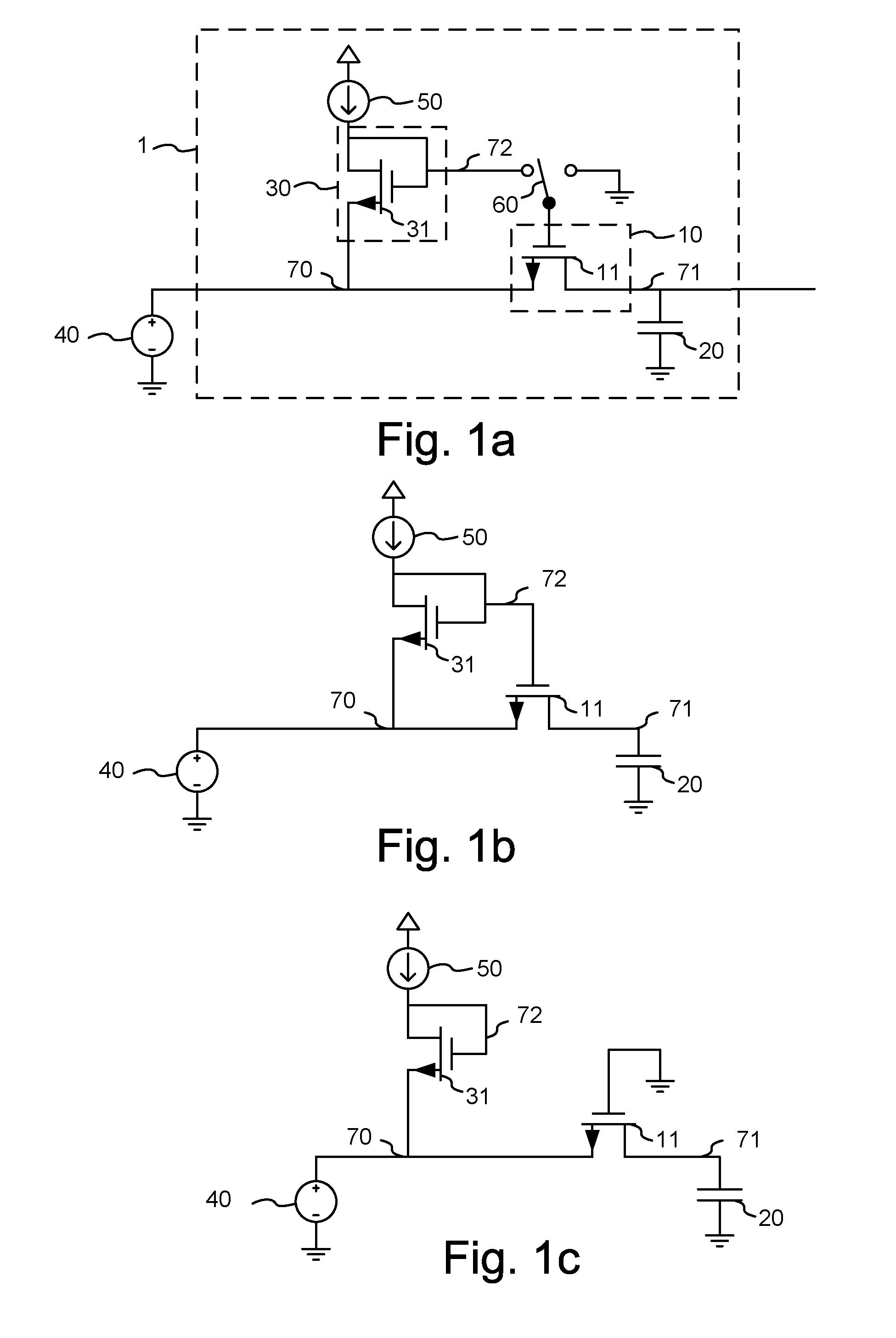
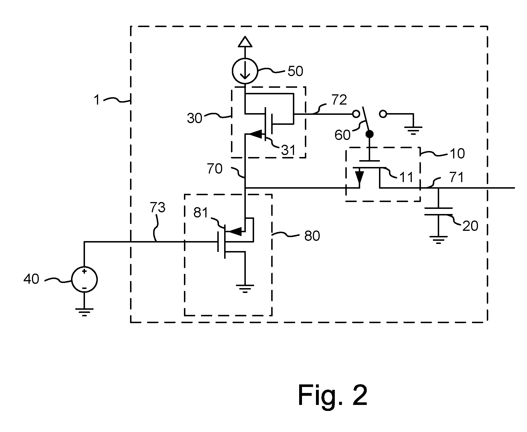
[0035]FIG. 1a shows an embodiment of a track and hold circuit 1. In the embodiment, a switch device 10 embodied with an NMOS transistor 11 is included. For the NMOS transistor 11, a first order approximation of the channel charge, QCH, is
QCH≈−WLCOX(VGS−VT)
where W is a channel width of the NMOS transistor 11, L is a channel length of the NMOS transistor 11, VGS is the gate-to-source voltage of the NMOS transistor 11, VT is the threshold voltage of the NMOS transistor 11, and COX is the gate-oxide capacitance per unit area of the NMOS transistor 11.
[0036]A first order approximation of the on resistance of the NMOS transistor 11 is
RON≈Lμ0COXW(VGS-VT)
where μ0 is an electron mobility for the NMOS transistor 11.
[0037]The track and hold circuit 1 further comprises a track-voltage generating device 30. The track-voltage generating device 30 may be adapted to track threshold voltage variations of the switch device 10 and to generate a control voltage for the switch device 10 during the track...
PUM
 Abstract
Description
Claims
Application Information
 - R&D
- Intellectual Property
- Life Sciences
- Materials
- Tech Scout
- Unparalleled Data Quality
- Higher Quality Content
- 60% Fewer Hallucinations
Browse by: Latest US Patents, China's latest patents, Technical Efficacy Thesaurus, Application Domain, Technology Topic, Popular Technical Reports.
© 2025 PatSnap. All rights reserved.Legal|Privacy policy|Modern Slavery Act Transparency Statement|Sitemap|About US| Contact US: help@patsnap.com


