Combi-Card and Method for Making the Same
a technology of combi-cards and cards, applied in the field of combi-cards and a method of making the same, can solve the problems of reducing durability, affecting the use of the same, and causing contact failure, etc., and achieves excellent adhesive strength, excellent adhesive strength, and good electrical conductivity.
- Summary
- Abstract
- Description
- Claims
- Application Information
AI Technical Summary
Benefits of technology
Problems solved by technology
Method used
Image
Examples
embodiment 1
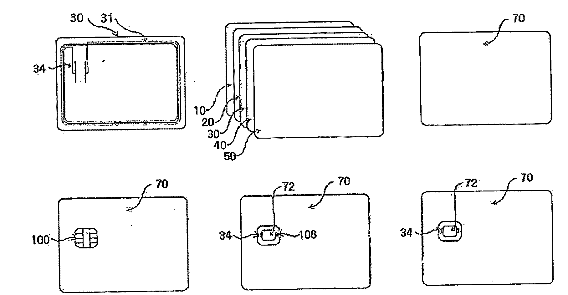
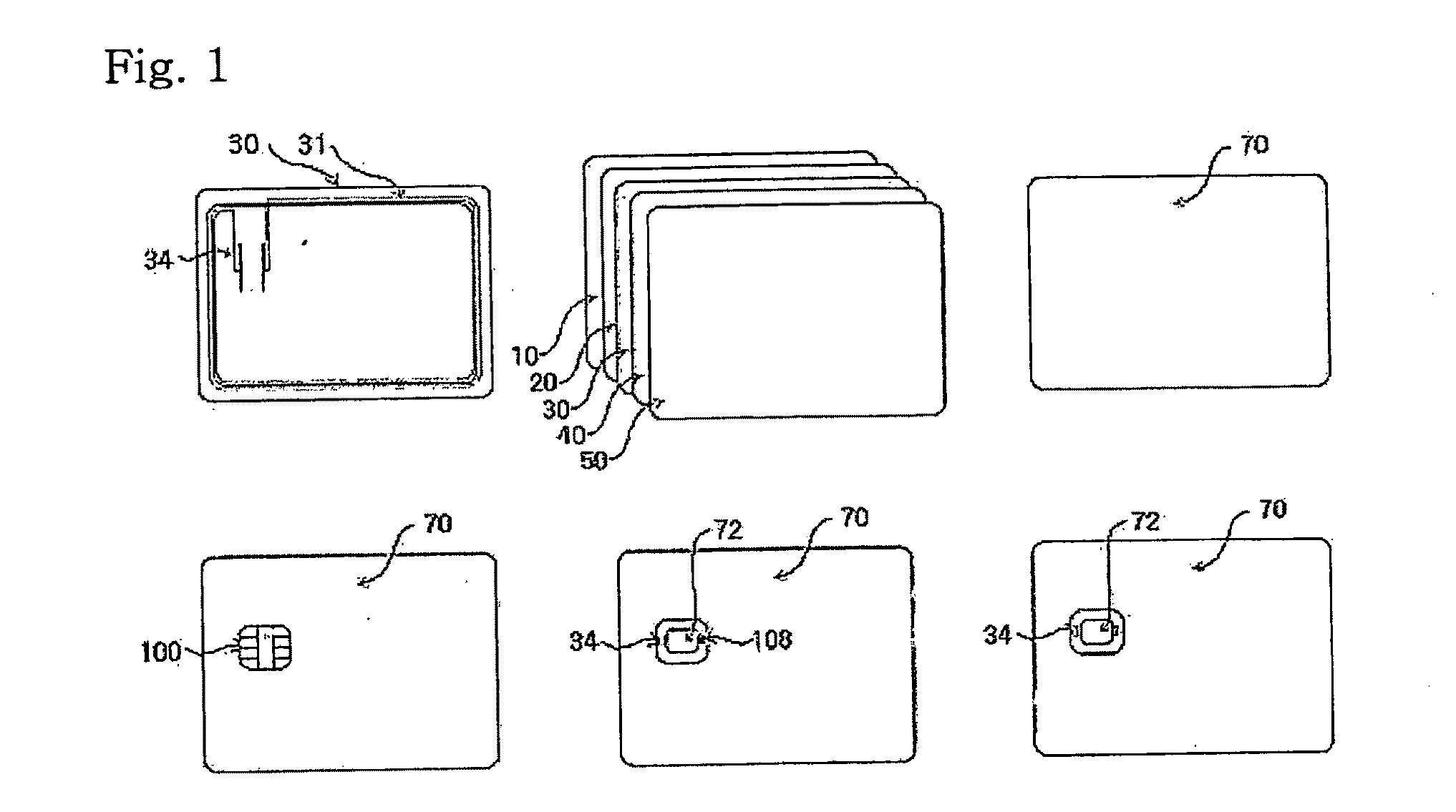
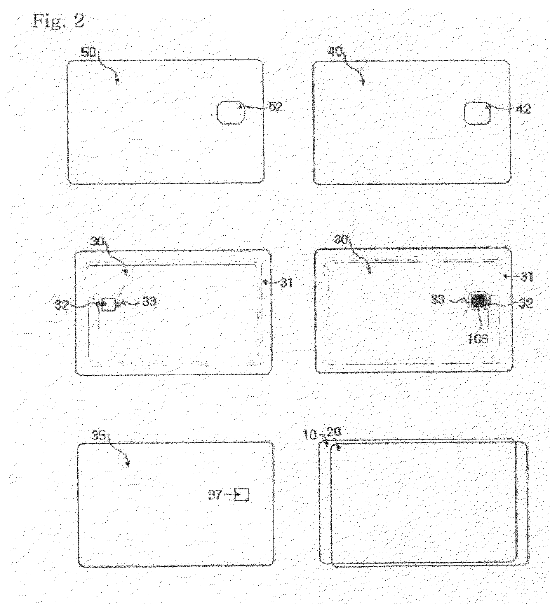
[0076]For a correct positioning of the COB 100 and the antenna coil insertion layer 30, as in FIG. 9, the respective two round-tipped pin bars 210 (each diameter is 5 mm or less and height is 5 mm or less) are set up on the top and bottom surfaces of the metal die 200, and the COB-shaped pit 220 is formed on a surface of the die 200, at a depth of 160-230 μm. The COB 100 is inserted into the pit 220, so that the ACF 112 pre-treated on the COB 100 can face up. Then, the dam positioning opening 32 of the antenna coil insertion layer 30, which is 100-250 μm thick and on which the conductive fiber antenna terminal 33 is formed, is aligned by using the pin bars 210, and thereafter, by applying heat and pressure, the COB 100 is provisionally adhered to the antenna coil insertion layer 30. By doing so, the sheet for antenna coil insertion, in which the ACF-applied COB contact 104 is adhered and electrically connected to the conductive fiber antenna terminal 33 directly, is formed as is sho...
embodiment 2
[0079]As shown in FIG. 3, the lower protection layer 10, which is 50-100 μm thick; the lower printing layer 20, which is 100-200 μm thick; the antenna coil thickness-adjusting layer 35, which is 100-250 μm thick and on which the COB dam positioning opening 37 is formed; the antenna coil insertion layer 30, which is 100-200 μm thick and on which the COB dam positioning opening 32 and the conductive fiber antenna terminal 33 are formed; the upper printing layer 40 which is 100-200 μm thick and on which the COB positioning opening 42 is formed; and the upper protection layer 50 which is 50-100 μm thick and on which the COB positioning opening 52 is formed, are in turn stacked upward. After the air and the static electricity between the respective layers has been removed by a roller, the COB 100, on which the ACF 112 is pre-treated, is inserted into the opening 72 to which the COB 100 will be secured. Then, by applying heat and pressure, the ACF-applied COB contact 104 is adhered and el...
PUM
| Property | Measurement | Unit |
|---|---|---|
| diameter | aaaaa | aaaaa |
| depth | aaaaa | aaaaa |
| height | aaaaa | aaaaa |
Abstract
Description
Claims
Application Information
 - R&D
- Intellectual Property
- Life Sciences
- Materials
- Tech Scout
- Unparalleled Data Quality
- Higher Quality Content
- 60% Fewer Hallucinations
Browse by: Latest US Patents, China's latest patents, Technical Efficacy Thesaurus, Application Domain, Technology Topic, Popular Technical Reports.
© 2025 PatSnap. All rights reserved.Legal|Privacy policy|Modern Slavery Act Transparency Statement|Sitemap|About US| Contact US: help@patsnap.com


