
Semiconductor device

a semiconductor and device technology, applied in the field of semiconductor devices, can solve the problems of difficult design of difficult to apply noise reduction techniques inapplicability to semiconductor devices having coc structures, etc., to improve the reliability of semiconductor devices, increase the overall electrostatic capacitance, and increase the overall layout area for aligning

Active Publication Date: 2009-07-30
LONGITUDE LICENSING LTD
View PDF7 Cites 16 Cited by
  • Summary
  • Abstract
  • Description
  • Claims
  • Application Information

AI Technical Summary

Benefits of technology

The invention provides a semiconductor device with a first semiconductor chip and even-numbered pairs of second semiconductor chips laminated above the first chip. The second semiconductor chips have a drive voltage electrode and a reference potential electrode connected to the first chip's electrodes. The second chips are activated and inactivated alternately. The inactivated chip's logic circuit is integrated with the activated chip's logic circuit, which increases the overall electrostatic capacitance and reduces feed noise. The invention improves the reliability of the semiconductor device.

Problems solved by technology

The present inventor has recognized that the above noise reduction technique suffers from the following problem and is not applicable to semiconductor devices having COC structures.
Generally speaking, it is difficult to design semiconductor devices having COC structures in consideration of severe requirements for reducing feed noises, wherein feed noises increase in response to increasing the currents consumed in semiconductor memories, and wherein noise margins decrease in response to decreasing the drive voltages in the recent developments of semiconductor manufacturing processes.
Since semiconductor devices having COC structures are designed to feed electric power to semiconductor chips in the order from the lowermost one to the uppermost one, semiconductor chips formed in lower layers have a high priority in feeding electric charge thereto; hence, it is difficult to feed electric charge to semiconductor chips formed in upper layers.
To solve the problem, it is necessary to increase electrostatic capacitances of on-chip capacitors mounted on semiconductor chips; but this increases the overall layout area for mounting semiconductor chips, thus pushing up manufacturing cost.

Method used


Image

  • Semiconductor device
  • Semiconductor device
  • Semiconductor device

Examples


first embodiment

1. First Embodiment

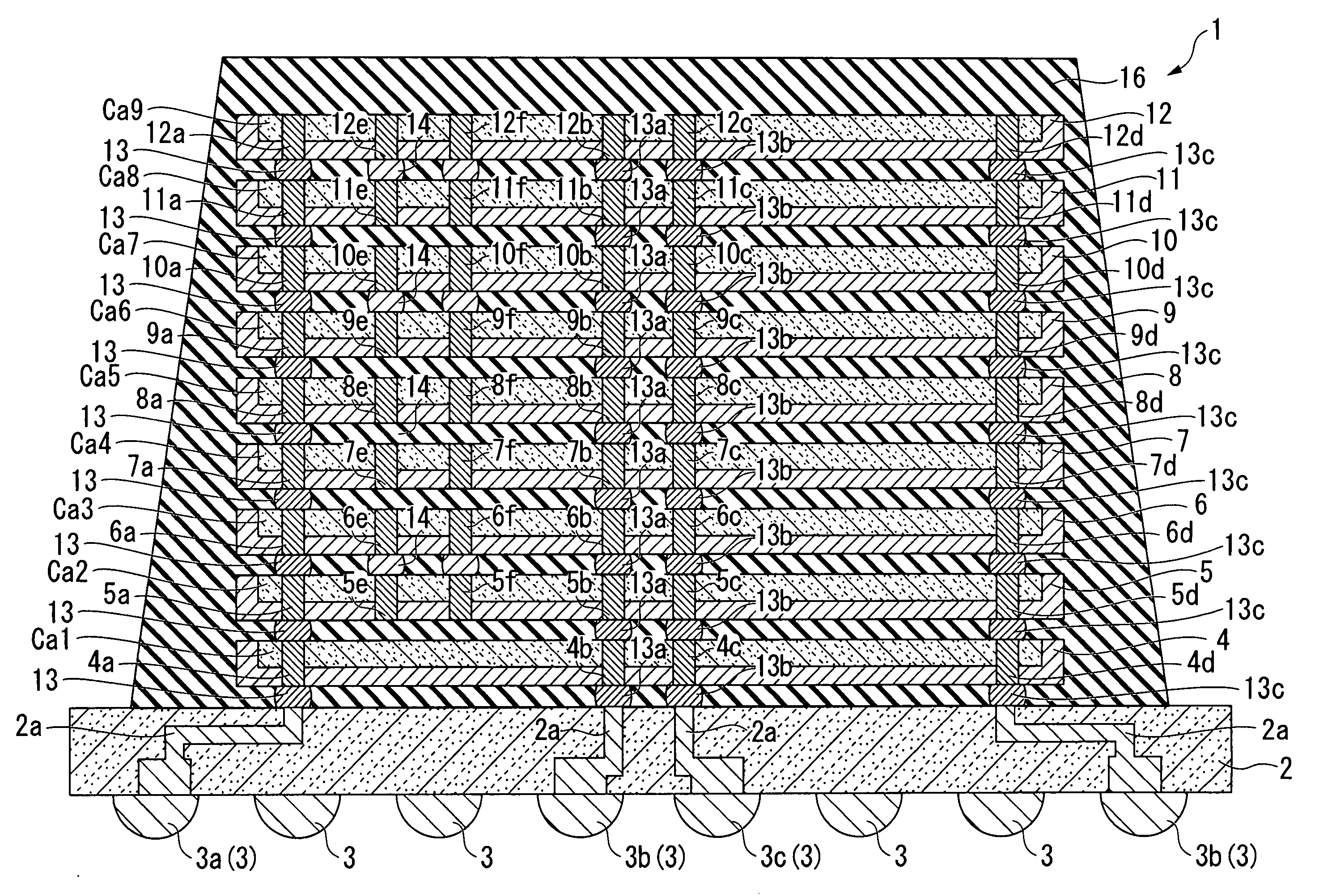
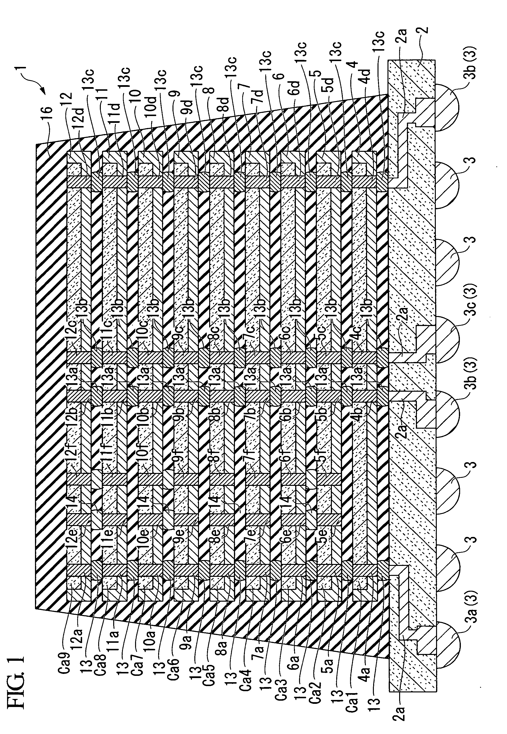
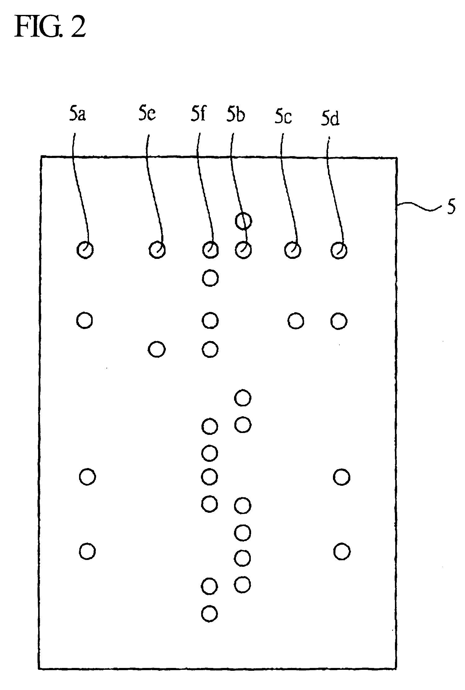
[0035]FIG. 1 is a cross-sectional view of a semiconductor device 1 according to a first embodiment of the present invention. FIG. 2 is a top view of a semiconductor chip used in the semiconductor device 1. FIG. 3 is a diagram used for explaining a controller selecting semiconductor chips included in the semiconductor device 1. FIG. 4 is a circuit diagram showing a first example of equivalent circuits of semiconductor chips included in the semiconductor device 1. FIG. 5 shows equivalent circuits of a semiconductor chip whose logic circuit does not operate. FIG. 6 shows equivalent circuits of a semiconductor chip whose logic circuit does not operate. FIG. 7 is a circuit diagram showing a second example of equivalent circuits of semiconductor chips included in the semiconductor device 1.

[0036]As shown in FIG. 1, the semiconductor 1 having a chip-on-chip (COC) structure is equipped with an interposer 2 (serving as a wiring substrate) having a plurality of connection e...

second embodiment

2. Second Embodiment

[0091]Next, a semiconductor device 100 according to a second embodiment of the present invention will be described with reference to FIGS. 8 to 12, wherein parts identical to those of the semiconductor device 1 are designated by the same reference numerals; hence, the duplicate descriptions thereof are simplified or omitted.

[0092]FIG. 8 is a cross-sectional view of the semiconductor device 100 according to the second embodiment of the present invention. FIG. 9 is a perspective view showing the laminated structure of the semiconductor chips 5 and 6 in the semiconductor device 100. FIG. 10 is a cross-sectional view taken along line A-A in FIG. 9. FIG. 11 is top view showing a first example of fabrication of through-vias and electrodes in the semiconductor chips 5 and 6. FIG. 12 is a top view showing a second example of fabrication of through-vias and electrodes in the semiconductor chip 5.

[0093]The semiconductor device 100 of the second embodiment is designed in a ...


PUM


Abstract

A semiconductor device having a chip-on-chip structure is constituted of a first semiconductor chip and even-numbered pairs of second semiconductor chips, all of which are laminated together on the surface of an interposer. The first semiconductor chip controls each pair of the second semiconductor chips so as to activate one second semiconductor chip while inactivating another second semiconductor chip. The second semiconductor chips are paired together in such a way that through-vias and electrodes thereof are positioned opposite to each other via bumps. Since drive voltage electrodes supplied with a drive voltage (VDD) and reference potential electrodes supplied with a reference potential (VSS) are mutually connected together between the paired second semiconductor chips, it is possible to increase the overall electrostatic capacitance of each second semiconductor chip so as to substantially reduce feed noise without increasing the overall layout area of the semiconductor device.

Description

BACKGROUND OF THE INVENTION[0001]1. Field of the Invention[0002]The present invention relates to semiconductor devices having chip-on-chip structures for three-dimensionally laminating semiconductor chips via on-chip capacitors. In particular, the present invention relates to techniques for reducing feed noises while increasing on-chip capacitances.[0003]The present application claims priority on Japanese Patent Application No. 2008-2536, the content of which is incorporated herein by reference.[0004]2. Description of Related Art[0005]Semiconductor memories having chip-on-chip (COC) structures have been developed to meet requirements for achieving high performance (e.g. for increasing storage capacities) and for size reduction (e.g. for improving packaging densities).[0006]A typical example of a semiconductor device having a chip-on-chip (COC) structure is designed to laminate a plurality of semiconductor memories (e.g. semiconductor chips serving as dynamic random-access memories) ...

Claims


Application Information

Patent Timeline
Patent Type & Authority Applications(United States)
IPC IPC(8): H01L23/522
CPCH01L23/49827H01L23/49838H01L23/50H01L25/0657H01L25/18H01L2224/16145H01L2224/16225H01L2225/06517H01L2225/06527H01L2225/06541H01L2924/15311H01L2924/01055H01L2225/06513H01L2224/05573H01L2224/13025H01L2924/00014H01L2224/0615H01L2224/0616H01L2224/05599
Inventor SUZUKI, EIICHIOSAKA, HIDEKIUEMATSU, YUTAKANISHIO, YOJI
Owner LONGITUDE LICENSING LTD
Learn More