Charging-free electron beam cure of dielectric material

a dielectric material and electron beam treatment technology, applied in the direction of calibration apparatus, optical radiation measurement, instruments, etc., can solve the problems of affecting the operation speed of the overall chip, the undesirable side effects of electron beam treatment on the front-end of the line device, and the tendency of ultra-low-k materials to crack, etc., to achieve the effect of reducing the undesirable charging effect of e-beam curing, increasing young's modulus and hardness

Inactive Publication Date: 2009-07-16
IBM CORP
View PDF14 Cites 3 Cited by
  • Summary
  • Abstract
  • Description
  • Claims
  • Application Information

AI Technical Summary

Benefits of technology

[0010]The present invention provides a novel method and tool design that alleviates the undesirable charging effects of e-beam curing, while preserving all its advantages, including increase in Young's modulus and hardness.
[0011]In the present invention, an ultra low-k dielectric material layer is formed on a semiconductor substrate. In one embodiment, a grid of wires is placed at a distance above a top surface of the ultra low-k dielectric material layer and is electrically biased such that the total electron emission coefficient becomes 1.0 at the energy of electrons employed in electron beam curing of the ultra low-k dielectric material layer. The shadowing effect of the grid of wires is compensated for by moving the grid of wires to make an average dose of electrons uniform across the ultra low-k dielectric material layer. In another embodiment, a polymeric conductive layer is formed directly on the ultra low-k dielectric material layer and is electrically biased so that the total electron emission coefficient becomes 1.0 at the energy of electrons employed in electron beam curing of the ultra low-k dielectric material layer. By maintaining the total electron emission coefficient at 1.0, charging of the substrate is avoided, thus protecting any device on the substrate from any adverse changes in electrical characteristics.

Problems solved by technology

In advanced semiconductor chips operating at frequencies above 1 GHz range, signal propagation delay between various devices or components in the semiconductor chip accounts for a significant fraction of overall chip operation speed.
While attempts to integrate various materials having a low dielectric constant, commonly referred to as “low-k materials” in the art, have produced some successful results in the art for materials having a dielectric constant of about 2.8 or greater, integration of ultra low dielectric constant (ultra low-k) material into the BEOL metallization faces several significant challenges.
Efforts to integrate ultra low-k materials into BEOL interconnect wiring structures demonstrated that the ultra low-k materials have a tendency to crack, especially at high humidity environments.
Unfortunately, an electron beam treatment has undesirable side effects on front-end of the line (FEOL) devices, e.g., field effect transistors (FETs).
Such effects include reduced break down voltage characteristics, large threshold voltage shifts, and other adverse effects attributed to charging of the substrate and various films on it, due to the electron beam.

Method used


Image

  • Charging-free electron beam cure of dielectric material
  • Charging-free electron beam cure of dielectric material
  • Charging-free electron beam cure of dielectric material

Examples


Embodiment Construction

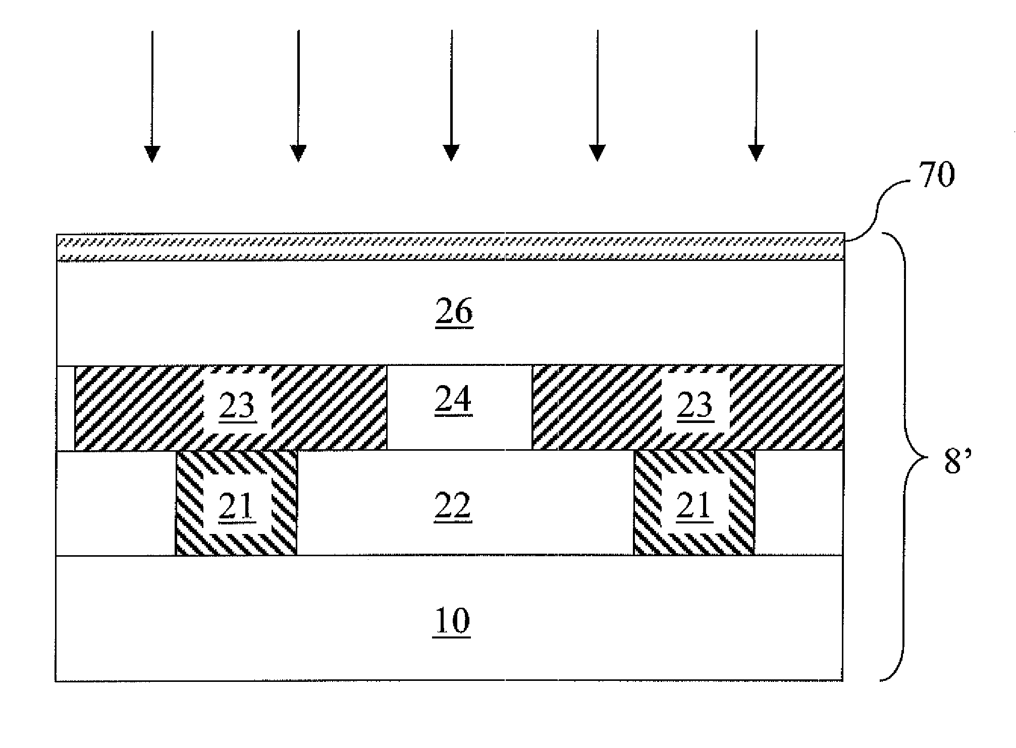
[0065]As stated above, the present invention relates to methods of electron beam curing of dielectric materials. It is noted that like and corresponding elements mentioned herein and illustrated in the drawings are referred to by like reference numerals.

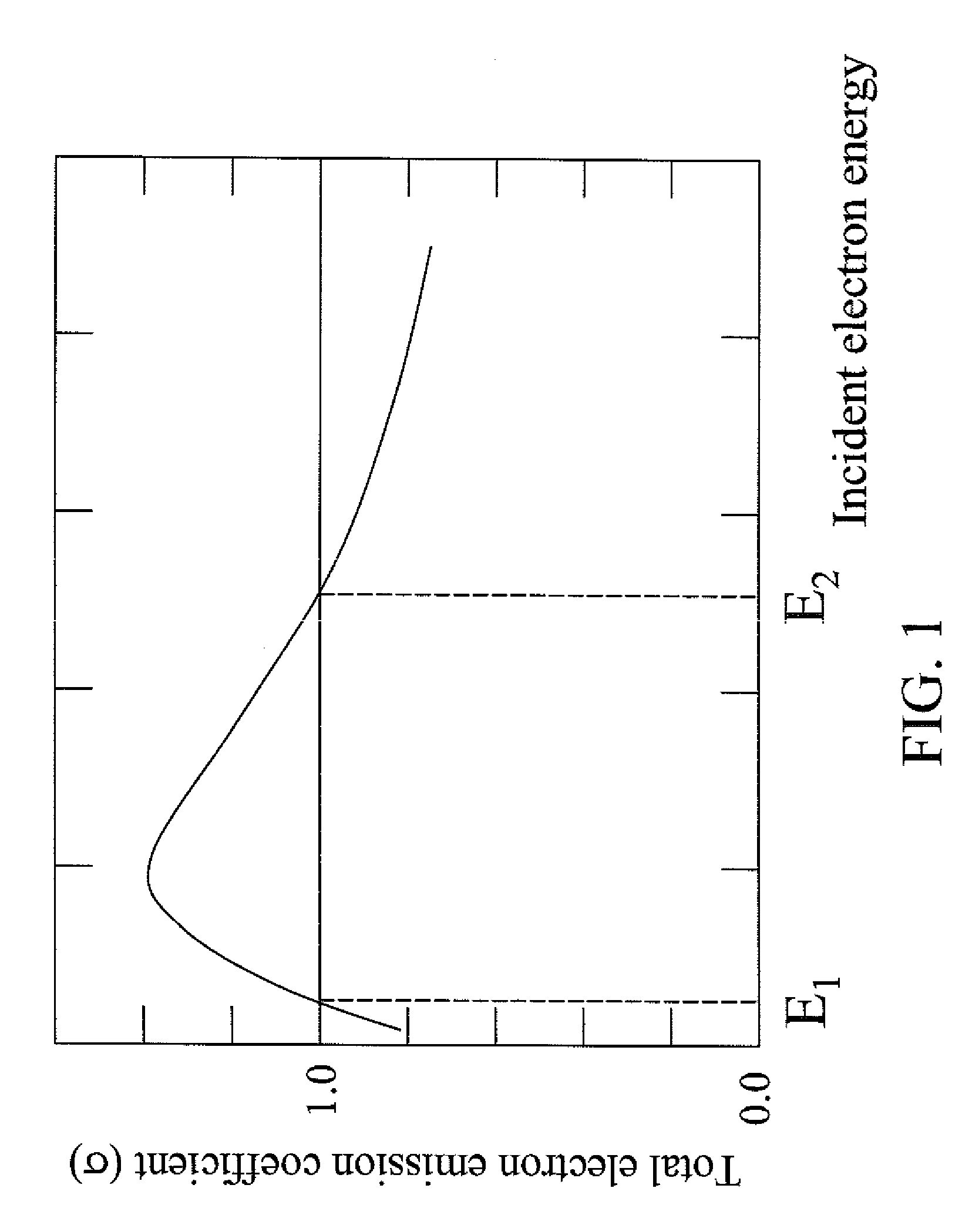
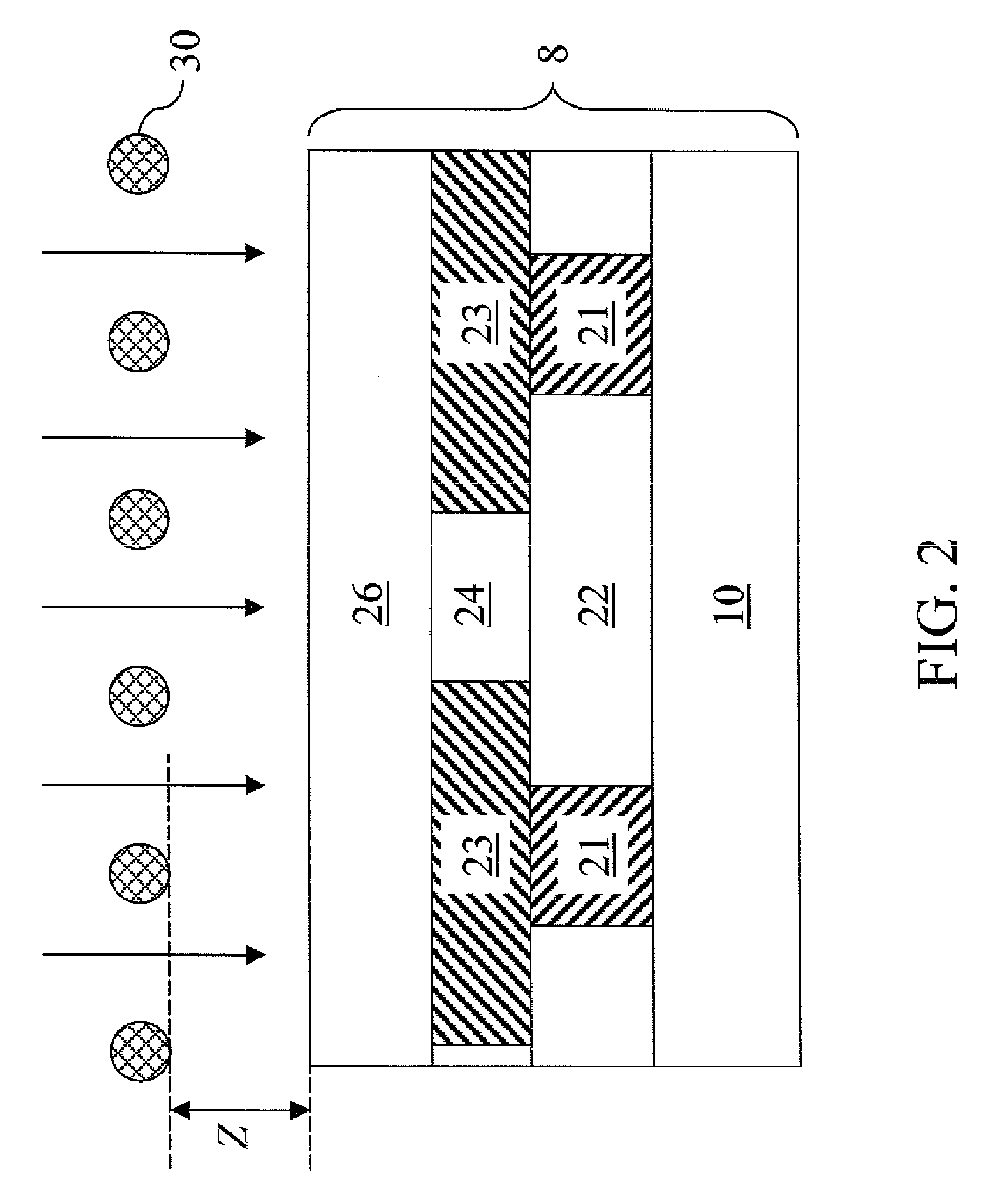
[0066]In the past, electron beams have been used to charge conducting pads and vias in a ceramic package in order to test their electrical conductor continuity (J. M. Engel and F. E. Holmstrom J. Phys. D 3, 1505, (1970); J. M. Sebeson J. Vac. Sci and Technol. 6, 1060, (1973); Pfeiffer et al. J. Vac. Sci and Technol. 19, 1014, (1981); Lee et al. J. Vac. Sci and Technol. B 9, 1993, (1991)). In one of the steps of this charging and testing method, a conducting grid placed in the proximity of a sample surface was used to induce repeatable charging of the sample. According to the present invention, a conducting grid placed in the proximity of a dielectric layer that is subjected to an e-beam cure is electrically biased in order to ensure ...


PUM

PropertyMeasurementUnit
dielectric constantaaaaaaaaaa
energyaaaaaaaaaa
frequenciesaaaaaaaaaa

Abstract

An ultra low-k dielectric material layer is formed on a semiconductor substrate. In one embodiment, a grid of wires is placed at a distance above a top surface of the ultra low-k dielectric material layer and is electrically biased such that the total electron emission coefficient becomes 1.0 at the energy of electrons employed in electron beam curing of the ultra low-k dielectric material layer. In another embodiment, a polymeric conductive layer is formed directly on the ultra low-k dielectric material layer and is electrically biased so that the total electron emission coefficient becomes 1.0 at the energy of electrons employed in electron beam curing of the ultra low-k dielectric material layer. By maintaining the total electron emission coefficient at 1.0, charging of the substrate is avoided, thus protecting any device on the substrate from any adverse changes in electrical characteristics.

Description

FIELD OF THE INVENTION[0001]The present invention generally relates to methods of manufacturing a semiconductor structure, and particularly to methods of electron beam curing of dielectric materials.BACKGROUND OF THE INVENTION[0002]In advanced semiconductor chips operating at frequencies above 1 GHz range, signal propagation delay between various devices or components in the semiconductor chip accounts for a significant fraction of overall chip operation speed. The signal propagation delay in an interconnect structure is dependent on an RC product of the interconnect structure, where R denotes the resistance of the interconnect wires and C denotes the interconnect capacitance, or the overall capacitance of the interconnect structure in which the interconnect wires are embedded. The continuous shrinking in dimensions of electronic devices utilized in ultra-large scale integration (ULSI) circuits in recent years has resulted in increase in the resistance of the back-end of the line (B...

Claims


Application Information

Patent Timeline
Patent Type & Authority Applications(United States)
IPC IPC(8): H01L21/4763B05C11/00
CPCB29C71/04B29C2035/0877H01J37/026H01J37/317H01J2237/0044H01L21/76835H01J2237/047H01J2237/3156H01L21/3105H01L21/76825H01J2237/024
Inventor DIMITRAKOPOULOS, CHRISTOS D.LEE, KAM L.WISNIEFF, ROBERT L.
Owner IBM CORP
Why Eureka
Try Eureka