Differential communication link with skew compensation circuit
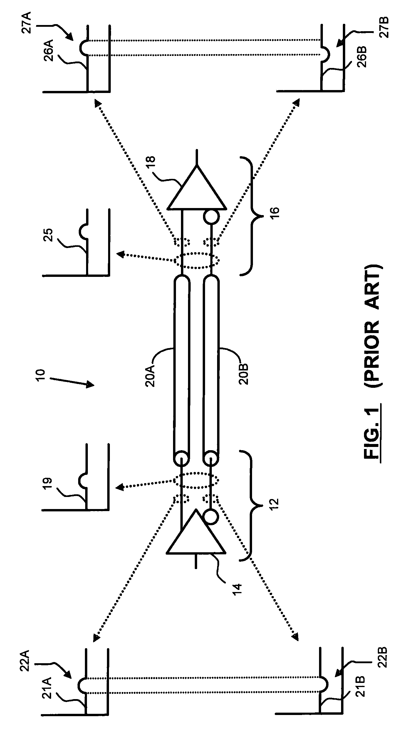
a communication link and compensation circuit technology, applied in the field of differential signal skew correction circuits, can solve the problems of increasing the size, complexity, cost of the circuit board, and the design methods of the computer-based circuit board design tools that do not employ these design methods, so as to minimize the relative skew, reduce the reflection of signals, and minimize the effect of skew
- Summary
- Abstract
- Description
- Claims
- Application Information
AI Technical Summary
Benefits of technology
Problems solved by technology
Method used
Image
Examples
first embodiment
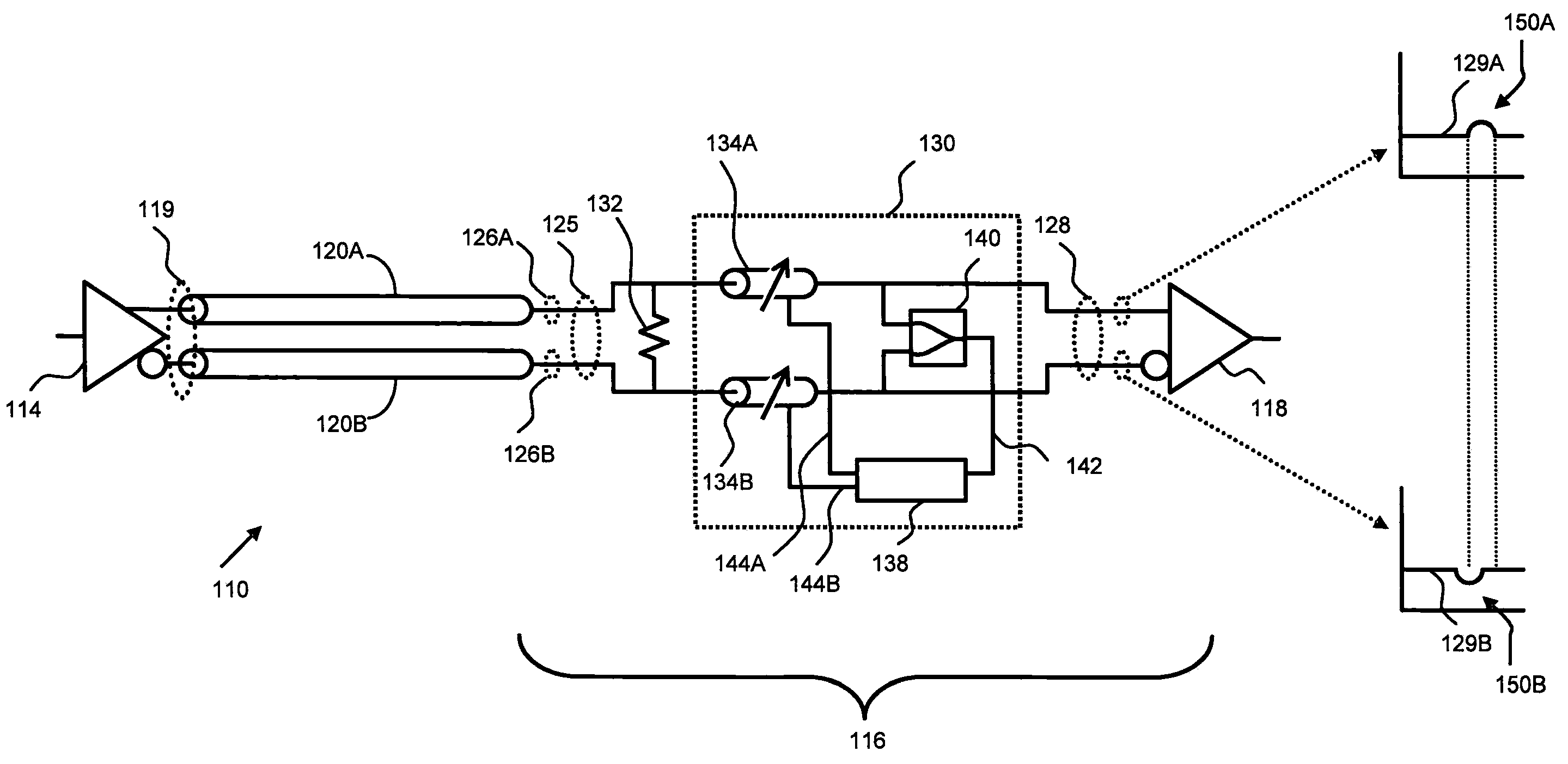
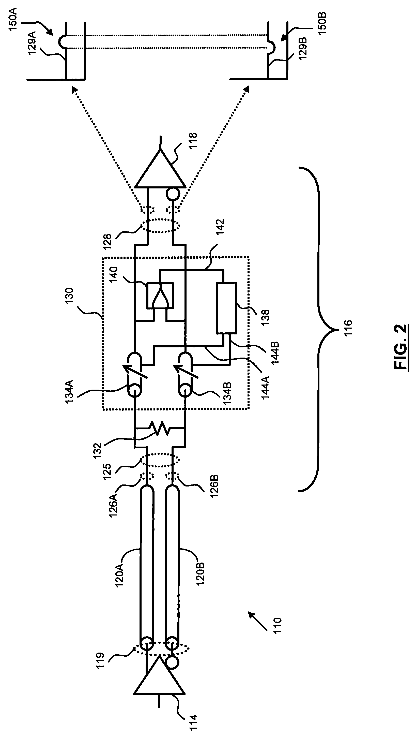
[0029]A high-speed differential signal communication link 110 according to the present invention is shown in FIG. 2. The communication link 110 includes a skew compensation circuit 130 disposed between a terminator 132 and a conventional differential signal receiver 118. A differential signal 119 generated by a conventional transmitter 114 is broadcast over a pair of differential transmission lines 120A, B in accordance with known systems and methods. The transmission lines 120A, B are terminated at the terminator 132 disposed in the receive end 116 of the link 110 to reduce signal reflections. Terminator 132 is shown as a single resistive element in FIG. 2, but those skilled in the art will recognize that transmission-line terminators can take many forms. The use of the term “terminator” is used herein to represent a circuit applied to the receive end 116 of a communication link 110 to provide optimal impedance match for minimizing signal reflections and / or optimizing the effective...
second embodiment
[0037]Turning now to FIG. 3, a high-speed differential signal communication link 210 according to the present invention is shown. The link 210 includes a skew compensation circuit 230 disposed between differential transmission lines 220A, B and a terminator 232. The configuration and operation of the skew compensation circuit 230 is similar to the circuit 130 of FIG. 2. The comparator skew detector 240, controller 238, and the delay elements 234A, B all operate in the same manner. However, the skew compensation circuit 230 is disposed upstream from a terminator 232 such that the effective input differential-impedance match into the skew compensation circuit 230 is enhanced by ensuring the received P-side and N-side signals 229A, B arrive simultaneously at the terminator, further improving the integrity of the differential signals 225.
third embodiment
[0038]Turning now to FIG. 4, a high-speed differential signal communication link 310 according to the present invention is shown. Like the high speed communication link 110 of FIG. 2, a skew compensation circuit 330 is disposed between a terminator 332 and a differential signal receiver 318. Unlike the links 110, 210 of FIGS. 2 and 3, no variable-delay elements are used in the skew compensation circuit 330 to compensate for skew in the differential signal.
[0039]As illustrated, the differential transmission lines 320A, B are terminated at the terminator 332 directed into the skew-compensation circuit 330. The circuit 330 is configured to detect and reduce relative skew occurring between the P-side and N-side signals 329A, B of the differential signal 328 that are subsequently fed into the differential receiver 318 at the receive end 316 of the link 310.
[0040]The skew detector 340 monitors the P-side and N-side signals 326A, B of the received differential signal 325 and quantifies the...
PUM
 Abstract
Description
Claims
Application Information
 - R&D
- Intellectual Property
- Life Sciences
- Materials
- Tech Scout
- Unparalleled Data Quality
- Higher Quality Content
- 60% Fewer Hallucinations
Browse by: Latest US Patents, China's latest patents, Technical Efficacy Thesaurus, Application Domain, Technology Topic, Popular Technical Reports.
© 2025 PatSnap. All rights reserved.Legal|Privacy policy|Modern Slavery Act Transparency Statement|Sitemap|About US| Contact US: help@patsnap.com


