Method for fabricating semiconductor device

Active Publication Date: 2009-07-02
SK HYNIX INC
View PDF6 Cites 10 Cited by
  • Summary
  • Abstract
  • Description
  • Claims
  • Application Information

AI Technical Summary

Benefits of technology

[0021]Various embodiments of the present invention are directed at providing a method for fabricating a semiconductor device that comprises forming a pattern for pad by applying an Anti-Reflection film before forming an etch target pattern by a cell mask process to improve profile and CD uniformity of the pattern for pad and to prevent scum of photo-resist patterns and pattern lifting, thereby improving characteristic of the device.

Problems solved by technology

However, these methods require development of new manufacturing equipment and cause difficulty in management of the equipment; and, thus, manufacturing cost is increased.
However, when an exposure process is performed, it is difficult to form a first fine photo-resist pattern defined in a mask by a difference in refractive indexes between a photo-resist film and the hard mask formed in the bottom of the photo-resist film.
As defocus of the peripheral region becomes worse, a manufacturing margin of depth of focus (DOF) is insufficient.
Furthermore, the sizes (widths) of the switching transistor and the selecting lines are larger than those of the control gates included in the cell string, so that it is difficult to form a fine pattern using the spacer 130.
However, the BARC film cannot be formed due to the previously formed spacer 130.
Also, the thickness of the photo-resist pattern 140 is required to increase, so that it is impossible to secure a process margin.
As a result, an etching selectivity is insufficient in etching the etch target layer 110.
As mentioned above, in the conventional method for fabricating a semiconductor device, it is difficult to apply an Anti-Reflection film in formation of the photo-resist pattern 140 having a pad type, which results in notching due to reflection of lights, in defects of the photo-resist pattern formed in the peripheral region, in scum in a narrow region between patterns and in pattern lifting due to degradation of adhesiveness with the substrate.

Method used


Image

  • Method for fabricating semiconductor device
  • Method for fabricating semiconductor device
  • Method for fabricating semiconductor device

Examples


Embodiment Construction

[0028]FIGS. 2a to 2g are cross-sectional diagrams illustrating a method for fabricating a semiconductor device according to an embodiment of the present invention. In the embodiment, the semiconductor device comprises a cell string connected to a plurality of control gates and a switching transistor for connecting a source selection line (SSL) and a drain selection line (DSL) at both ends of the cell string.

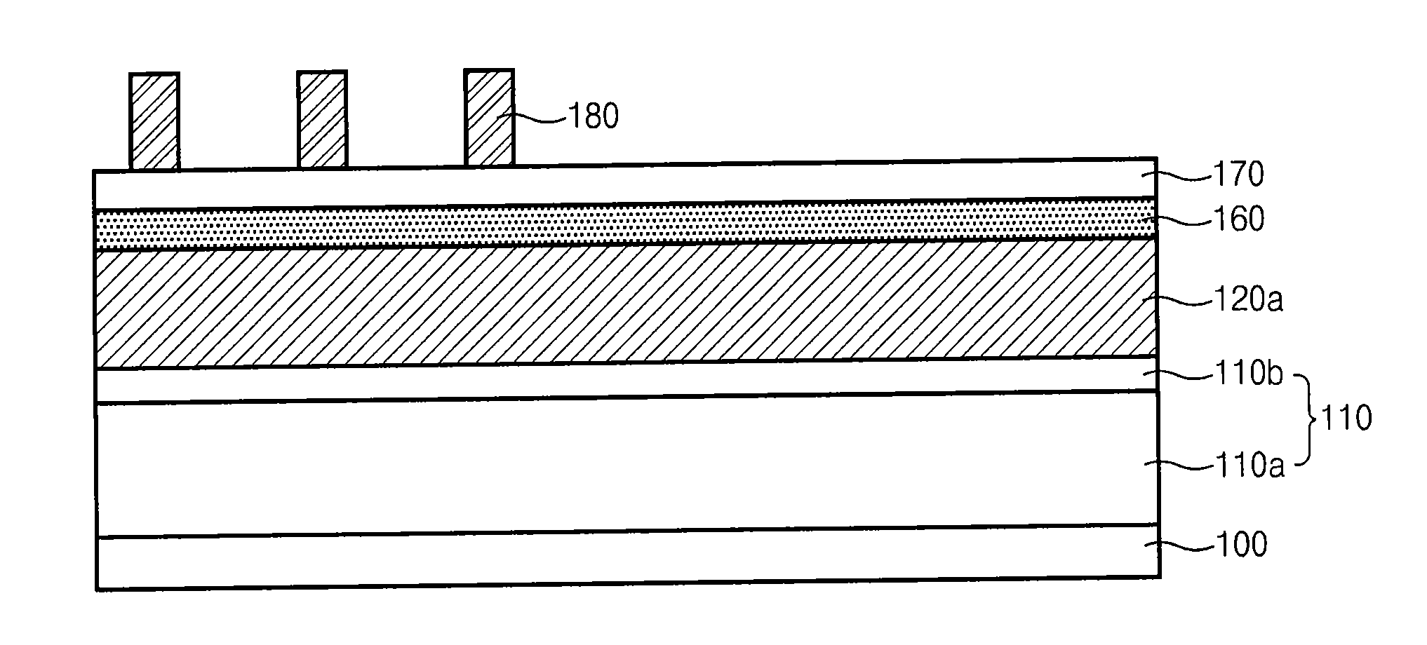
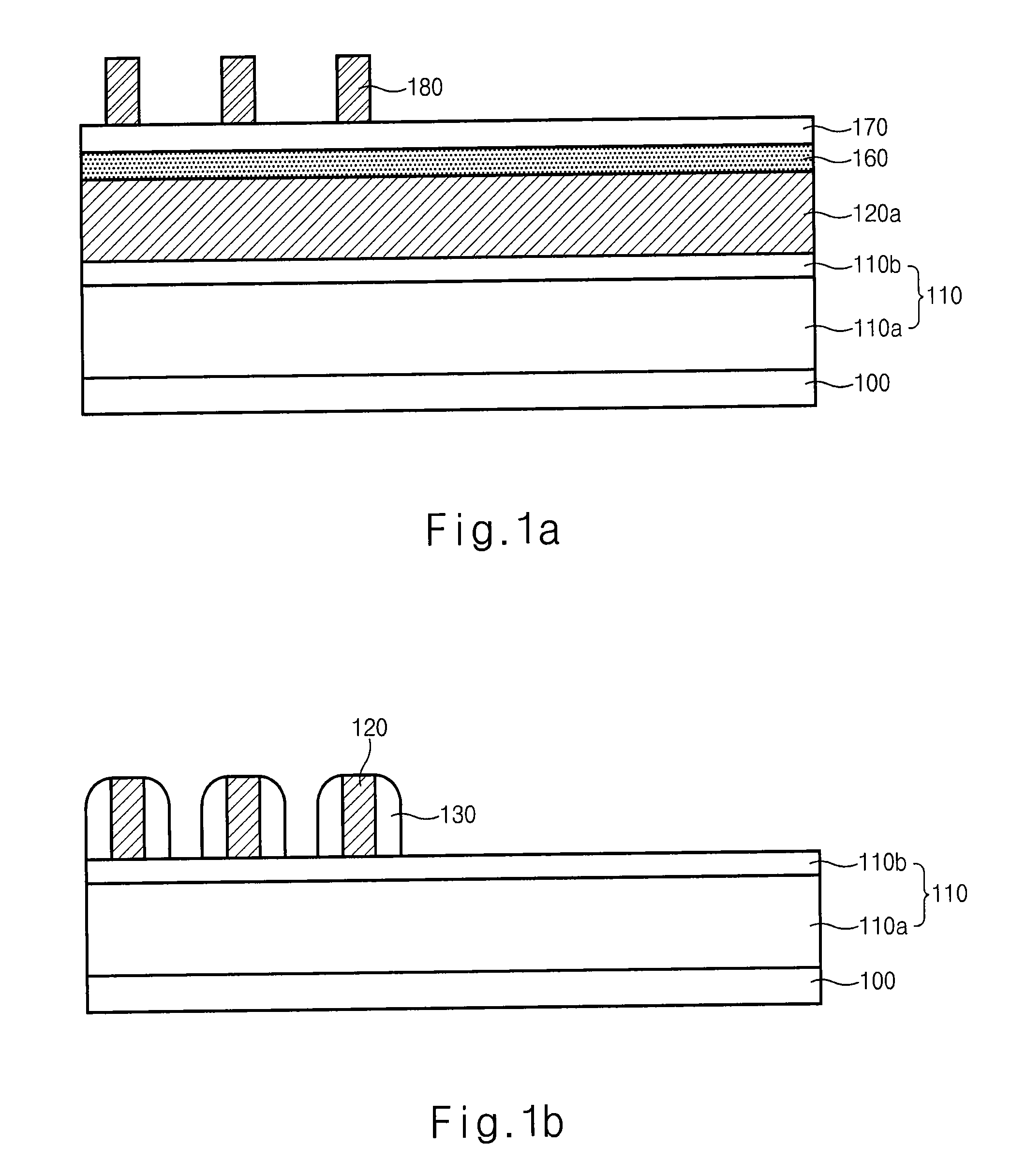
[0029]Referring to FIG. 2a, an etch target layer 210 is formed over a semiconductor substrate 200. A polysilicon layer 220a and a first BARC film 250a are formed over the etch target layer 210. A first photo-resist pattern 260a that defines a pattern for pad is formed over the first BARC film 250a. The etch target layer 210 has a deposition structure including a polysilicon 210a and a nitride film 210b.

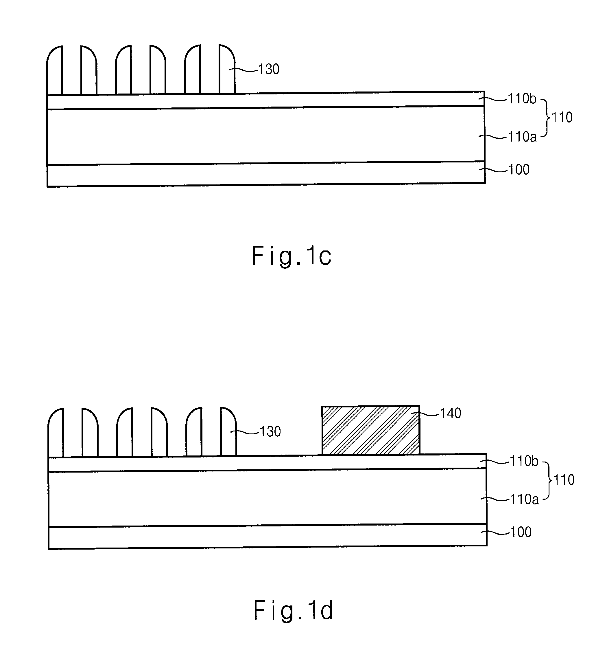
[0030]Referring to FIG. 2b, the polysilicon layer 220a is etched with the first photo-resist pattern 260a as a mask to form a pattern 220 for pad that defines a gate of the switch...


PUM


Abstract

A method for fabricating a semiconductor device includes forming a first mask pattern over an etch target layer, forming a second mask pattern over the etch target layer, forming spacers at sidewalls of the first mask pattern and the second mask pattern, and etching the etch target layer with an etching mask where the second mask pattern is removed. The method improves a profile of a pad pattern and critical dimension uniformity.

Description

CROSS-REFERENCES TO RELATED APPLICATIONS[0001]Priority to Korean patent applications numbers 10-2007-0140859 and 10-2008-49895, filed on Dec. 28, 2007 and May 28, 2008 respectively, which are incorporated by reference in its entirety, is claimed.BACKGROUND OF THE INVENTION[0002]The present invention relates to a method for fabricating a semiconductor device using a spacer patterning technology (SPT).[0003]As the degree of integration of semiconductor devices has increased, the size and pitch of patterns that form circuits have been reduced. For forming a fine pattern in the semiconductor device, various manufacturing equipments and process methods have been suggested.[0004]Photo lithography process (also called optical lithography) is a process used in micro fabrication to selectively remove parts of a thin film (or the bulk of a substrate). It uses light to transfer a geometric pattern from a photo mask to a light-sensitive chemical (photo-resist, or simply “resist”) on the substra...

Claims


Application Information

Patent Timeline
IPC IPC(8): H01L21/302H01L21/02H01L21/20
CPCH01L21/0337H01L27/11524H01L27/11521H01L21/28273H01L29/40114H10B41/30H10B41/35
Inventor LEE, KI LYOUNGBOK, CHEOL KYU
Owner SK HYNIX INC
Why Eureka
Try Eureka