
Heterostructure device and associated method

a heterostructure device and heterostructure technology, applied in the direction of semiconductor devices, basic electric elements, electrical apparatus, etc., can solve the problems of low on-state resistance of the channel, high electron mobility, and may not be practical or desirable in switching devices

Inactive Publication Date: 2009-06-04
GENERAL ELECTRIC CO
View PDF8 Cites 6 Cited by
  • Summary
  • Abstract
  • Description
  • Claims
  • Application Information

AI Technical Summary

Benefits of technology

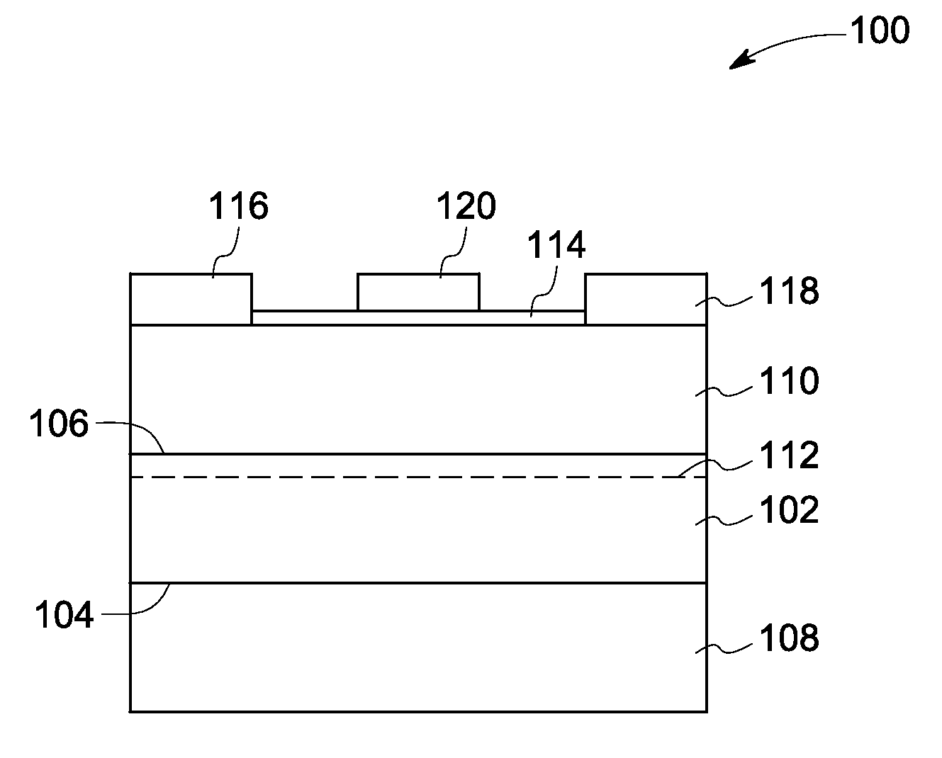
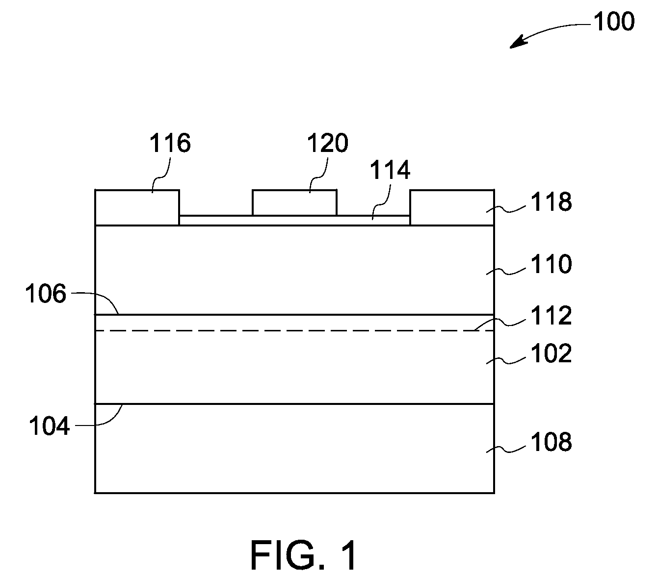
[0006]In accordance with an embodiment of the invention, an article is provided that includes a carrier transport layer, a back channel layer and a barrier layer. The carrier transport layer has a first surface and a second surface opposing to the first surface. The back channel layer is secured to the first surface of the carrier transport layer and the barrier layer is secured to the second surface of the carrier transport layer. Each of the carrier transport layer, the back channel layer and the barrier layer comprises an aluminum gallium nitride alloy. The article further includes a 2D electron gas at an interface of the second surface of the carrier transport layer and a surface of the barrier layer. The 2D electron gas is defined by a bandgap differential at an interface allowing electron mobility. In one embodiment, a system is provided that includes a heterostructure field effect transistor that includes the article.

Problems solved by technology

The junction may create a thin layer where the Fermi energy level is above the conduction band, giving the channel very high electron mobility and leading to low on-state resistance for the channel.
Such HFETs may not be practical or desirable in switching devices, such as inverters or converters.

Method used


Image

  • Heterostructure device and associated method
  • Heterostructure device and associated method
  • Heterostructure device and associated method

Examples


example 1

Forming Normally-Off Heterostructure Field Effect Transistors

[0053]Two normally-off aluminum gallium nitride based heterostructure field effect transistors (HFET) are formed. In both structures, a back channel layer is formed from a 1-micrometer thick epilayer having a composition of Al0.1Ga0.9N. The back channel layer is formed on a sapphire substrate. A 30-Angstrom thick carrier transport layer is epitaxially grown on the back channel layer. The carrier transport layer includes Al0.01Ga0.99N. A 50-Angstrom thick barrier layer is epitaxially grown on the carrier transport layer. The barrier layer includes Al0.15Ga0.85N. A 200-Angstrom thick dielectric layer is formed on a portion of the barrier layer. The dielectric layer includes silicon dioxide and is deposited by low-pressure chemical vapor deposition (LPCVD) at 300 degrees Centigrade.

[0054]The first of the two structures has source and drain Ohmic contact pads formed by using an ion implantation method. The other of the two str...

example 2

Effect of Thickness and Concentration on Threshold Voltage

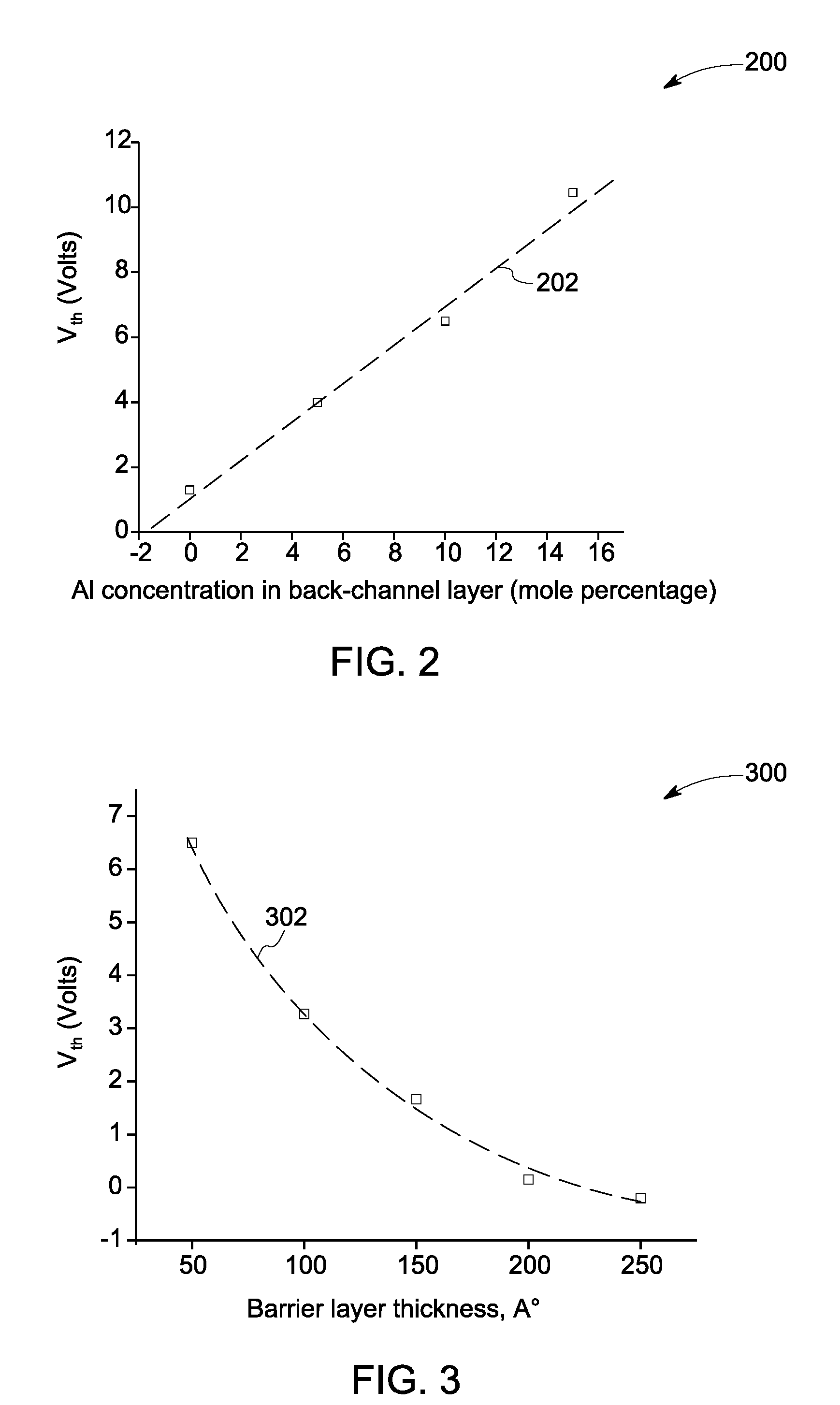
[0056]Two sets of 3 samples are created in a manner similar to the devices formed in Example 1; except that the samples have the values listed in Table 1. The values for each of the first set and the second set are the same as each other except that the first set (1A, 2A, 3A) involves ion implantation for the contact pads, and the second set (1B, 2B, 3B) involves reversibly electrically isolating the contact pads by a physical removal of material to define a recess.

[0057]As indicated by data, controlling the thickness and aluminum concentrations of the layers control the threshold voltage. The aluminum concentration ‘y’ of the carrier transport layer is less than the aluminum concentration ‘z’ of the barrier layer to lead an increase in the density of 2D electron gas. However, by controlling the concentration of the back channel layer less than the aluminum concentration of the barrier layer provides positive threshold voltag...


PUM


Abstract

A heterostructure device or article includes a carrier transport layer, a back channel layer and a barrier layer. The carrier transport layer has a first surface and a second surface opposing to the first surface. The back channel layer is secured to the first surface of the carrier transport layer and the barrier layer is secured to the second surface of the carrier transport layer. Each of the carrier transport layer, the back channel layer and the barrier layer comprises an aluminum gallium nitride alloy. The article further includes a 2D electron gas at an interface of the second surface of the carrier transport layer and a surface of the barrier layer. The 2D electron gas is defined by a bandgap differential at an interface, which allows for electron mobility. A system includes a heterostructure field effect transistor that includes the article.

Description

TECHNICAL FIELD[0001]The invention includes embodiments that relate to a semiconductor heterostructure device. The invention includes embodiments that relate to a method of making and / or using the power semiconductor device.DISCUSSION OF RELATED ART[0002]A semiconductor material for high power applications may need good thermal properties, high breakdown voltage, chemical inertness, mechanical stability and the ability to be fabricated as either a unipolar device or a bipolar device. Some currently available semiconductor materials for use as a power device may include silicon or gallium arsenide.[0003]A field-effect transistor (FET) may rely on an electric field to control the conductivity of a “channel” that is defined in the semiconductor material. A FET, like all transistors, may be thought of as a voltage-controlled current source. Some FETs may use a single-crystal semiconductor wafer as the channel, or active region. A terminal in a FET may be one of a gate, a drain, or a sou...

Claims


Application Information

Patent Timeline
Patent Type & Authority Applications(United States)
IPC IPC(8): H01L29/778
CPCH01L29/7786H01L29/2003
Inventor VERTIATCHIKH, ALEXEIMATOCHA, KEVIN SEANSANDVIK, PETER MICAHTILAK, VINAYAKRAJAN, SIDDHARTHCHA, HO-YOUNG
Owner GENERAL ELECTRIC CO
Learn More