Bandgap reference voltage generation circuit in semiconductor memory device

a reference voltage and memory device technology, applied in the direction of digital storage, process and machine control, instruments, etc., can solve the problems of large layout area, difficult to control the output level independent of temperature characteristics, complicated fabrication process,

Inactive Publication Date: 2009-05-14
SK HYNIX INC
View PDF4 Cites 37 Cited by
  • Summary
  • Abstract
  • Description
  • Claims
  • Application Information

AI Technical Summary

Benefits of technology

[0009]Embodiments of the present invention are directed to providing a bandgap reference voltage generation circuit in a semiconductor memo

Problems solved by technology

However, since a conventional bandgap reference voltage generation circuit using the CTAT characteristics of the base-emitter (Vbe) of the BJT basically uses both the BJT and MOSFET, its fabrication process is complicated and its layout area is large.
Moreover, when the conventional bandgap reference voltage generation circuit intends to generate

Method used


Image

  • Bandgap reference voltage generation circuit in semiconductor memory device
  • Bandgap reference voltage generation circuit in semiconductor memory device
  • Bandgap reference voltage generation circuit in semiconductor memory device

Examples


Embodiment Construction

[0013]Hereinafter, a bandgap reference voltage generation circuit in a semiconductor memory device in accordance with the present invention will be described in detail with reference to the accompanying drawings.

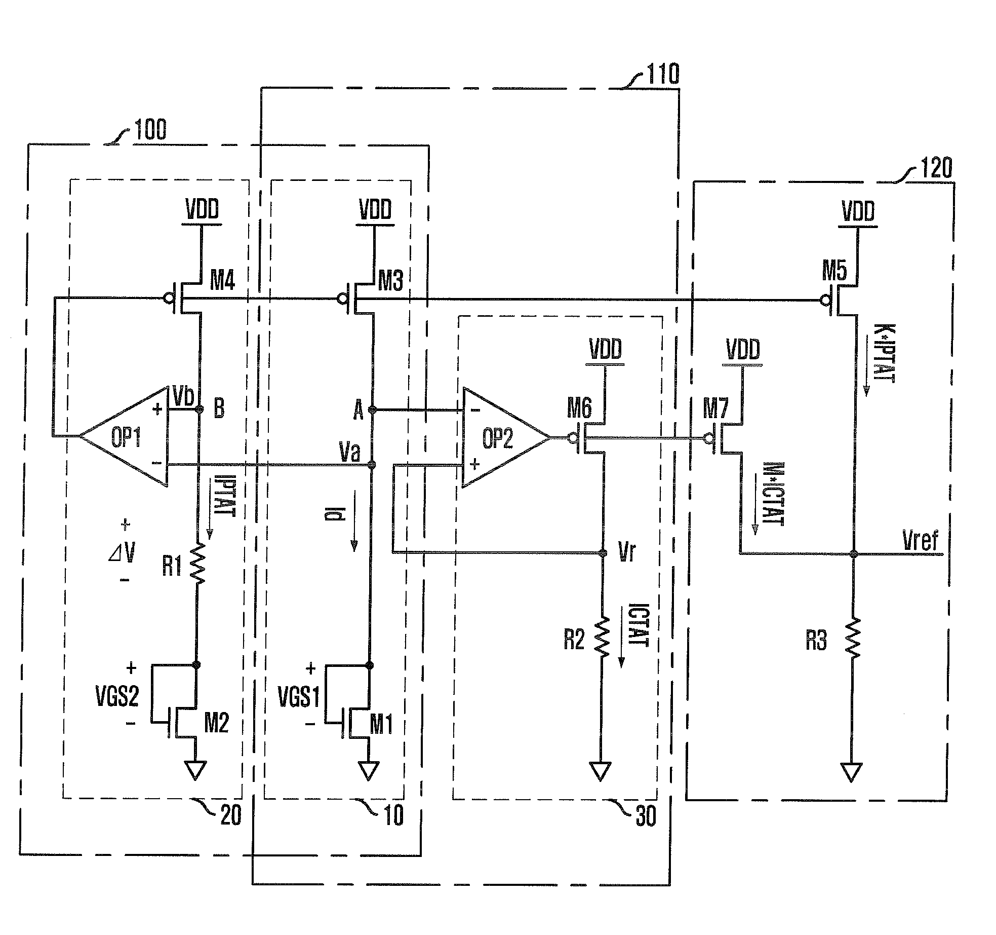
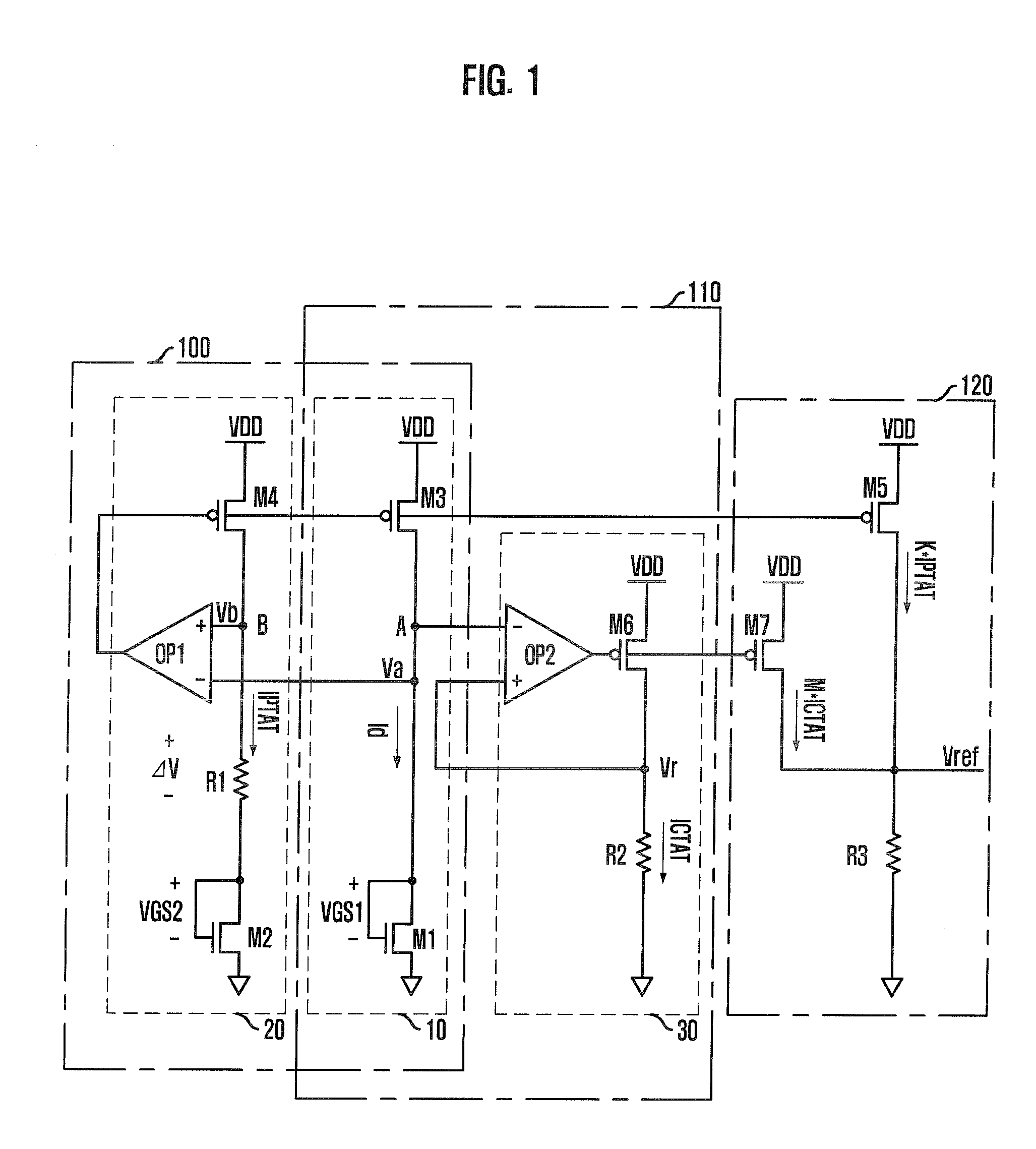
[0014]FIG. 1 is a circuit diagram of a bandgap reference voltage generation circuit in a semiconductor memory device in accordance with one embodiment of the present invention.

[0015]Referring to FIG. 1, a bandgap reference voltage generation circuit in accordance with one embodiment of the present invention includes a first current generator 100, a second current generator 110, and a summation unit 120. The first current generator 100 generates a current IPTAT proportional to the change of a temperature by using the temperature characteristic of a diode-connected NMOS transistor. The second current generator 110 generates a current ICTAT inversely proportional to the change of a temperature by using the temperature characteristic of a diode-connected NMOS transistor. The sum...


PUM


Abstract

Bandgap reference voltage generation circuit in semiconductor memory device includes a first current generator configured to generate a first current proportional to a change of a temperature by using temperature characteristic of a diode-connected MOS transistor, a second current generator configured to generate a second current inversely proportional to the change of the temperature by using the temperature characteristic of a diode-connected MOS transistor and a summation unit configured to mirror and sum the output currents of the first current generator and the second current generator, and output a reference voltage.

Description

CROSS-REFERENCES TO RELATED APPLICATIONS[0001]The present invention claims priority of Korean patent application numbers 10-2007-0113664, filed on Nov. 8, 2007, which is incorporated by reference in their entirety.BACKGROUND OF THE INVENTION[0002]The present invention relates to a semiconductor design technology, and more particularly, to an internal voltage generation circuit of a semiconductor memory device. More specifically, the present invention relates to a bandgap reference voltage generation circuit.[0003]A semiconductor memory device generates a variety of internal voltages using an external power voltage (VDD) and a ground voltage (VSS). A dynamic random memory access (DRAM), which is a representative semiconductor memory device, internally generates a core voltage (VCORE) used as a voltage level corresponding to data ‘1’ in a memory core region, a high voltage (VPP) used as a word ling enabling voltage of a cell transistor, and a back bias voltage (VBB) used as a bulk bia...

Claims


Application Information

Patent Timeline
IPC IPC(8): G05F3/16
CPCG05F3/30G11C5/147G11C7/04G11C11/4074G11C2207/2227
Inventor PARK, JAE-BOUMBYEON, SANG-JIN
Owner SK HYNIX INC
Why Eureka
Try Eureka