Multi-layer circuit board and method of making the same
a multi-layer circuit board and circuit board technology, applied in the direction of dielectric characteristics, electric connection formation of printed elements, electric apparatus casings/cabinets/drawers, etc., can solve the problem that the known multi-layer circuit board cannot meet the recent demand for neither can electronic parts be formed on front and rear surface regions, etc. problems, to achieve the effect of high-density surface mounting of electronic parts, simplified manufacturing process, and low melting poin
- Summary
- Abstract
- Description
- Claims
- Application Information
AI Technical Summary
Benefits of technology
Problems solved by technology
Method used
Image
Examples
referential example 1
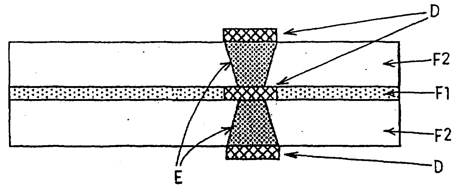
[0092]A thermoplastic liquid crystal polymer composed of a copolymer of p-hydroxybenzoic acid and 6-hydroxy-2-naphthoic acid and having a melting point of 283° C. was melt-extruded and then drawn by means of the inflation technique, wherein the draw ratio was 2.0 and the blow ratio was 6.0, to give a thermoplastic liquid crystal polymer film F1 of 20 μm in thickness and having a segment orientation ratio (SOR) of 1.03, a melting point of 283° C. and a thermal deformation temperature of 260° C.
referential example 2
[0093]A thermoplastic liquid crystal polymer composed of a copolymer of p-hydroxybenzoic acid and 6-hydroxy-2-naphthoic acid and having a melting point of 325° C. was melt-extruded and then drawn by means of the inflation technique, wherein the draw ratio was 2.0 and the blow ratio was 6.0, to give a thermoplastic liquid crystal polymer film F2 of 50 μm in thickness and having a segment orientation ratio (SOR) of 1.03, a melting point of 325° C. and a thermal deformation temperature of 305° C.
example 1
[0094]The multi-layer circuit board was obtained by the following procedures 1 to 4, which are shown respectively as FIGS. 10A to 10D.
Procedure 1:
[0095]A micro-via of a designed diameter of 100 μm was formed in the thermoplastic liquid crystal polymer film F2, obtained by the Referential Example 2, at a predetermined portion by means of a carbon dioxide laser. Thereafter, the micro-via was filled with an electroconductive paste which was subsequently cured by a preliminary heating (FIG. 10A).
Procedure 2:
[0096]An electrolytic copper foil of 18 μm in thickness was applied on each of the opposite surfaces of the thermoplastic liquid crystal polymer film F2 having the micro-via obtained by the Procedure 1. Then the stack (copper foil / thermoplastic liquid crystal polymer film / copper foil) was thermo compressed together at a temperature of 335° C. under a pressure of 3 MPa by a vacuum heat-press, to give the double-sided copper clad laminate in which the electroconductive paste filled in ...
PUM
| Property | Measurement | Unit |
|---|---|---|
| Temperature | aaaaa | aaaaa |
| Melting point | aaaaa | aaaaa |
| Thickness | aaaaa | aaaaa |
Abstract
Description
Claims
Application Information
 - R&D
- Intellectual Property
- Life Sciences
- Materials
- Tech Scout
- Unparalleled Data Quality
- Higher Quality Content
- 60% Fewer Hallucinations
Browse by: Latest US Patents, China's latest patents, Technical Efficacy Thesaurus, Application Domain, Technology Topic, Popular Technical Reports.
© 2025 PatSnap. All rights reserved.Legal|Privacy policy|Modern Slavery Act Transparency Statement|Sitemap|About US| Contact US: help@patsnap.com


