Variable slit device, illumination device, exposure apparatus, exposure method, and device manufacturing method
a technology of illumination light and variable slit, which is applied in the direction of photomechanical equipment, instruments, printers, etc., can solve the problem of predetermined time required to control illumination non-uniformity in illumination light,
- Summary
- Abstract
- Description
- Claims
- Application Information
AI Technical Summary
Benefits of technology
Problems solved by technology
Method used
Image

Examples
first embodiment
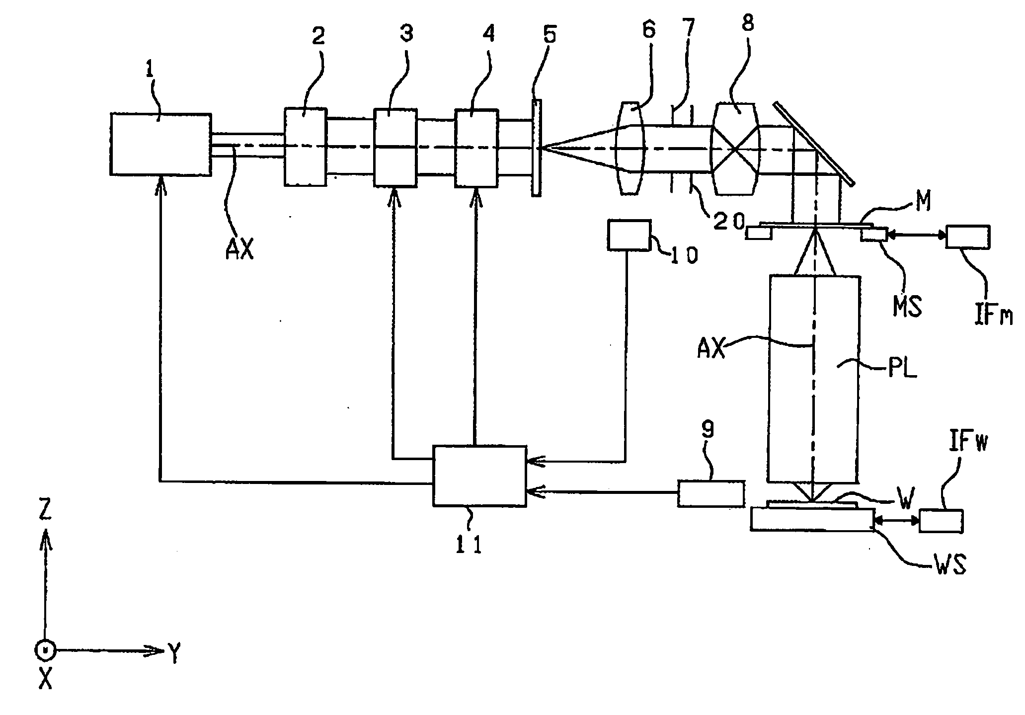
[0040]Embodiments of an exposure apparatus according to the present invention are described hereinafter with reference to the drawings. FIG. 1 is a diagram showing the structure of an exposure apparatus according to a In the following description, the XYZ orthogonal coordinate system is set as shown in FIG. 1, and the positional relationships of the various members is described with reference to this orthogonal coordinate system. The XYZ orthogonal coordinate system is set so that the X axis and the Y axis are parallel to a wafer W, and the Z axis is set in a direction that intersects the wafer W. In this embodiment the direction of movement (scanning direction) of a mask M and the wafer W is set in the X axis direction.
[0041]As shown in FIG. 1, the exposure apparatus of the first embodiment includes a light source 1, which supplies exposure light (illumination light). For example, an ArF excimer laser light source, which supplies light at a wavelength of approximately 193 nm, or a...
second embodiment
[0080]According to the exposure method of the second embodiment, when the second light intensity distribution is selected, the slit shape can be quickly changed to a slit shape which has the second light intensity distribution and accurate exposure can be a accomplished with a high throughput because the setting of the second light intensity distribution which corresponds to the second pattern group is executed simultaneously with the transfer of the first pattern group onto the wafer.
[0081]Although exposure is accomplished using a mask which has a first pattern group formed in a first pattern region and a second pattern group formed in a second pattern region in the exposure method of the second embodiment, exposure may also be accomplished using masks which separately form the first pattern group and the second pattern group. Although double exposure has been described in the exposure method of the second embodiment, the present invention is applicable to exposures other than doub...
fifth embodiment
[0094]FIG. 16(a) shows a shot array on a wafer w in the In FIG. 16(a), a plurality of shot regions (representatively indicated by shot regions A1 to A6) are formed at a predetermined pitch in the X direction and the Y direction on the wafer W.
[0095]As indicated by the arrows in FIG. 16(a), after the exposure apparatus exposes the wafer W at the shot region A1 while the wafer W is moved (scanned) in the −Y direction, the wafer W undergoes stepping in the −X direction. Then, the wafer W is exposed at the shot region A2 while the wafer W is moved (scanned) in the +Y direction. In the same manner, exposure is performed at the remaining shot regions while the wafer W is moved (scanned) in the +Y direction or −Y direction.
[0096]When variations in a synchronism accuracy error of a reticle and wafer occur depending on the scanning direction (+Y direction, −Y direction), the distribution of line width uniformity in the shot regions A1, A3, and A5, which are exposed by performing scanning in...
PUM
| Property | Measurement | Unit |
|---|---|---|
| wavelength | aaaaa | aaaaa |
| wavelength | aaaaa | aaaaa |
| diameter | aaaaa | aaaaa |
Abstract
Description
Claims
Application Information
 - R&D
- Intellectual Property
- Life Sciences
- Materials
- Tech Scout
- Unparalleled Data Quality
- Higher Quality Content
- 60% Fewer Hallucinations
Browse by: Latest US Patents, China's latest patents, Technical Efficacy Thesaurus, Application Domain, Technology Topic, Popular Technical Reports.
© 2025 PatSnap. All rights reserved.Legal|Privacy policy|Modern Slavery Act Transparency Statement|Sitemap|About US| Contact US: help@patsnap.com