Device and process for growing ga-doped single silicon crystals suitable for making solar cells

a technology of silicon crystals and solar cells, which is applied in the direction of crystal growth process polycrystalline material growth, etc., can solve the problems of no prior art method achieving such accurate straight gas delivery, speeding up crystallization, and reducing production costs, so as to facilitate large-scale industrial production and simplify the procedure

Inactive Publication Date: 2009-03-19
REN BING YAN +1
View PDF10 Cites 14 Cited by
  • Summary
  • Abstract
  • Description
  • Claims
  • Application Information

AI Technical Summary

Benefits of technology

[0006]One object of the present invention is to provide a device used for growing a silicon single crystal doped with Ga using a pulling method. Comparing with prior art devices, the device of the present invention is characterized in (a) having a shorter Φ16″ heater with an effective heating height between 300 mm and 375 mm while it is between 400 mm and 450 mm in the prior art and (b) having a funnel-shaped gas flow guide for directing an inert gas flowing directly towards the interface between the nascent crystal ingot and the melt of polycrystalline silicone raw material. The rim of the lower opening of the gas flow guide is positioned about less than 30 mm, preferably less than 25 mm, above the surface of the melt. By comparison, conventional methods all position the lower opening rim of the gas guide at least 45 mm above the surface of the melt. In addition, the present invention calls for the use of a Ga preparation with a 99.999999% purity, and direct burring of the Ga preparation into the polycrystalline silicon raw material during the charging process for proper doping without the need for preparing dopant in advance, hence simplifying the procedure, lowering production costs and enabling large scale industrial productions.
[0007]The shorter heater of the present invention offers the following advantages: First, the longitudinal temperature gradient of the melt is reduced effectively, which helps minimize the thermal convection within the melt. As a result, fewer impurities will come off from the inner wall of the quartz crucible into the melt due to the thermal convection. Second, the reduced longitudinal temperature gradient helps keep the melt calm, thereby creating such a physical condition at the crystallization frontier that is conducive to rapid crystallization. Third, the reduced longitudinal temperature gradient and thermal convention help reduce Ga segregation and ensure high doping rate and crystallization speed.
[0008]The use of a funnel-shaped gas flow guide also has the following advantages: First, the funnel shaped guide assists in directing the inert gas flow (such as Ar) from the top of the furnace effectively towards the nascent silicone single crystal ingot just coming out of the melt, thereby properly increasing the cooling rate and thermal gradient of the silicone single crystal ingot. This increases the growth rate of the ingot. Second, the funnel shaped gas flow guide can deliver the inert gas straight to the crystallization frontier where the outer surface of the nascent ingot interfaces with the surface of the melt. This speeds up the crystallization and shortens the ingot production cycle. No prior art method can achieve such accurate straight gas delivery. Third, the straight gas delivery to the crystallization frontier can reduce Ga segregation and ensure Ga integration in the ingot from the melt of the raw materials. This in turn reduces the difference of resistivity between the head portion and the tail portion of the ingot.
[0009]Another object of the present invention is to provide a method of fabricating large diameter silicon single crystals doped with Ga. The method is based on the CZ method, producing a Ga doped silicon single crystal having a diameter between 150 mm-165 mm and small resistivity deference between the head portion and tail portion suitable for being used in solar cells. The resistivity range of the silicon single crystal produced according to the present invention is between 3 Ω·cm-0.5 Ω·cm. Such result cannot be achieved by conventional pulling methods. By comparing with the prior art methods, the method according to the present invention is characterized by (a) using a higher inert gas flow rate in the heating chamber before melting the polycrystalline silicon raw material (for example, the Ar flow rate is adjusted to 20-35 L / h, which is about twice as high as conventionally used), and (b) using a slower rotation speed of the quartz crucible during the melting process of the raw material (the rotation speed is adjusted to 1-2 rpm while it is 3-5 rpm in prior art methods). These novel production conditions help reduce the resistivity difference between the head portion and the tail portion of arge diameter Ga doped silicon single crystals.

Problems solved by technology

This speeds up the crystallization and shortens the ingot production cycle.
No prior art method can achieve such accurate straight gas delivery.
This in turn reduces the difference of resistivity between the head portion and the tail portion of the ingot.
Such result cannot be achieved by conventional pulling methods.

Method used


Image

  • Device and process for growing ga-doped single silicon crystals suitable for making solar cells
  • Device and process for growing ga-doped single silicon crystals suitable for making solar cells
  • Device and process for growing ga-doped single silicon crystals suitable for making solar cells

Examples


Embodiment Construction

The Heating Device:

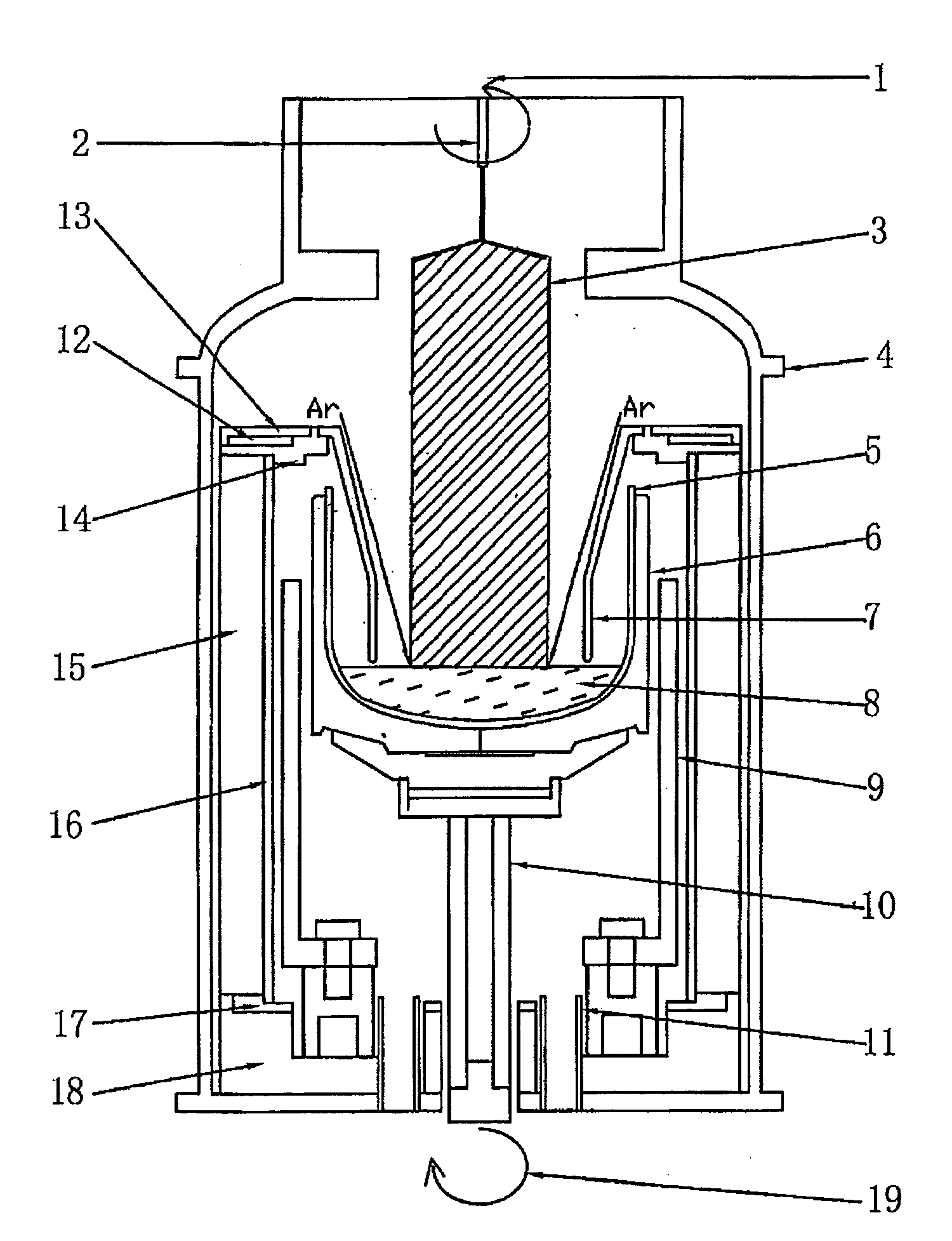
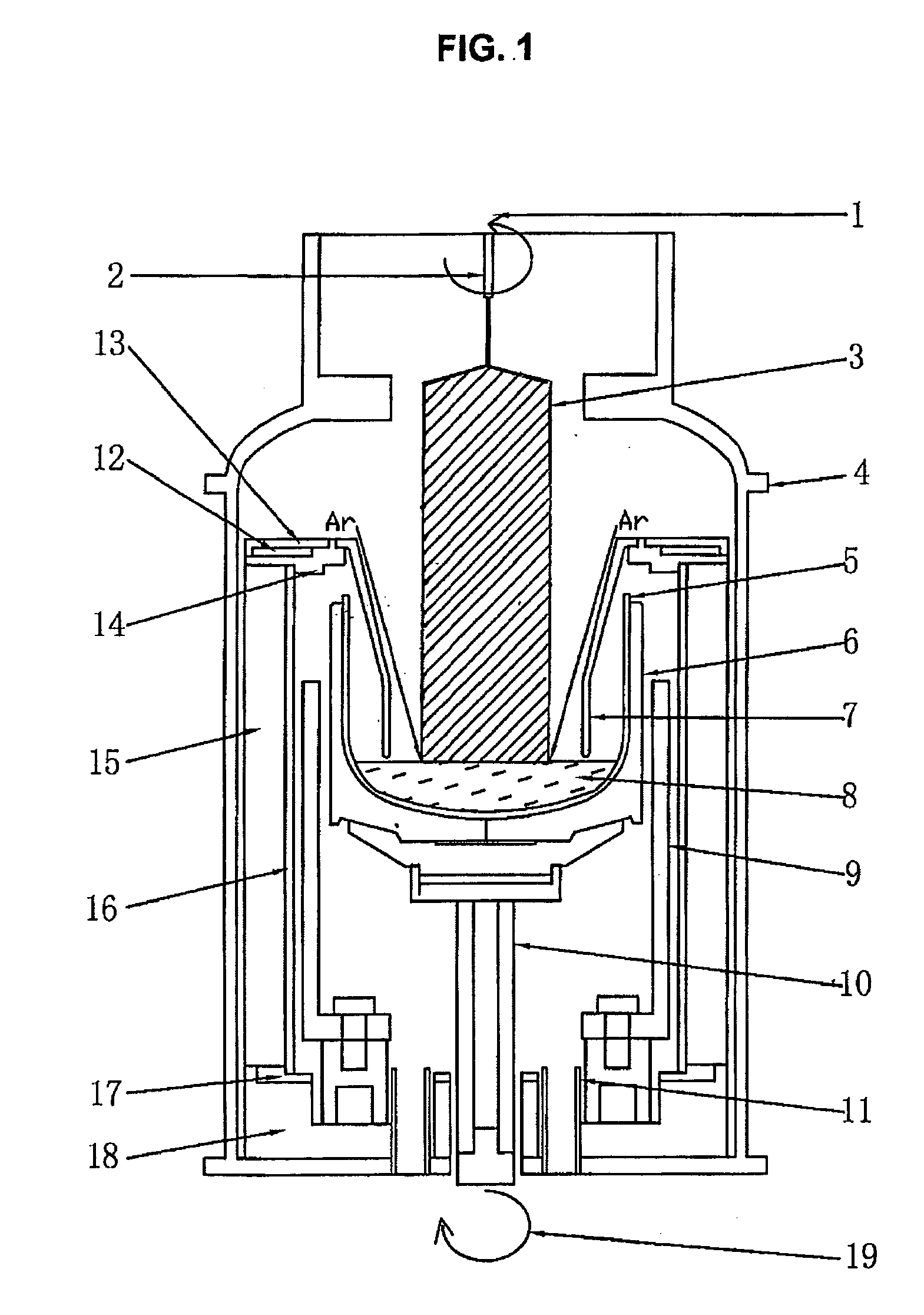
[0020]FIG. 1 depicts an exemplary heating device, of a furnace type, according to the resent invention, and it includes outer enclosure 4, quartz crucible 5, graphite crucible 6, multi-layered gas flow guide 7, heater 9, a shaft 10 supporting the graphite crucible, gas outlets 11, insulation carbon felt 12 and 15, insulation lid 13, upper position tray 14, lower position tray 17, graphite heat insulation tube 16 (which is about 15 mm distanced from the outer surface of the heater's sidewall), bottom tray 18 (see also FIG. 7). FIG. 1 also shows the heating device in operation, where there is a nascent silicon single crystal 3 growing out of the melt 8, and arrows 1 and 19 indicate that the nascent silicon single crystal ingot and the crucibles are rotating in the opposite directions.

[0021]The inner diameter of the chamber of the furnace or heating device is 620˜700 mm. The quartz crucible sits in the graphite crucible with the upper rim of the quartz crucible being...


PUM


Abstract

A device and method for producing Ga doped silicone single crystal with a diameter between 150 and 165 mm and a narrow resistivity distribution range (from 3 Ω·cm to 0.5 Ω·cm). The device is characterized by the use of a shorter heater and a funnel shaped gas flow guide capable of blowing an inert gas such as Ar straight to the crystallization frontier at the interface between outer surface of the nascent single crystal ingot and the surface of the melt of polycrystalline silicone raw materials in a quartz crucible.

Description

CROSS REFERENCE TO RELATED APPLICATIONS[0001]This application claims priority to Chinese Patent Application No. 200710058315.1, filed Jul. 15, 2007, the contents of which are hereby incorporated by reference.FIELD OF THE INVENTION[0002]This invention relates to a technique for manufacturing large diameter single silicon crystal doped with Ga using a CZ method (or pulling method) and more particularly, it relates to a device and process for growing silicon single crystal doped with Ga which has a resistivity distribution range sufficiently narrow to meet the requirement for fabricating silicon crystal solar cells.BACKGROUND OF THE INVENTION[0003]There are a number of domestic and foreign reported studies about resistivity distribution and characteristics of the silicon single crystal doped with Ga. For example, Pei, Su Hua et al. have disclosed a diffusion model and distribution principle of Ga in SiO2 / Si system (see Rare Metals and Material Engineering 2005, 6, pages 920-923). They ...

Claims


Application Information

Patent Timeline
IPC IPC(8): C30B15/14H01B1/04
CPCC30B15/14Y10T117/1052C30B29/06C30B15/206
Inventor REN, BING YANREN, LI
Owner REN BING YAN
Why Eureka
Try Eureka