
MEMS structure and optical modulator having temperature compensation layer

Inactive Publication Date: 2009-03-12
SAMSUNG ELECTRO MECHANICS CO LTD
View PDF3 Cites 12 Cited by
  • Summary
  • Abstract
  • Description
  • Claims
  • Application Information

AI Technical Summary

Benefits of technology

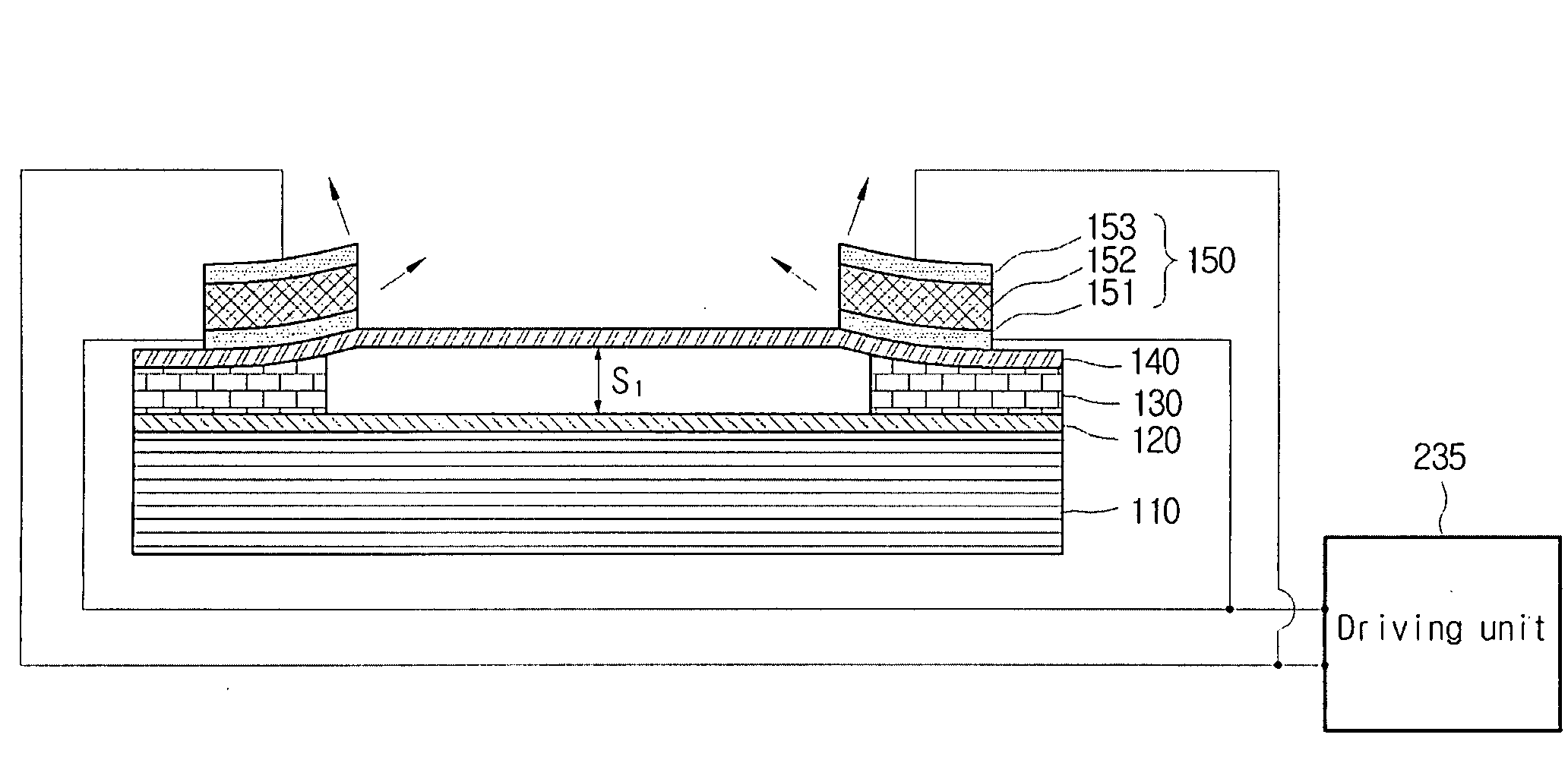
[0013]Another aspect of the invention is to provide a MEMS structure and optical modulator having a temperature compensation layer, in which the problem of thermal deformation is resolved, so that the accuracy and reliability of operation of the component are increased.

Problems solved by technology

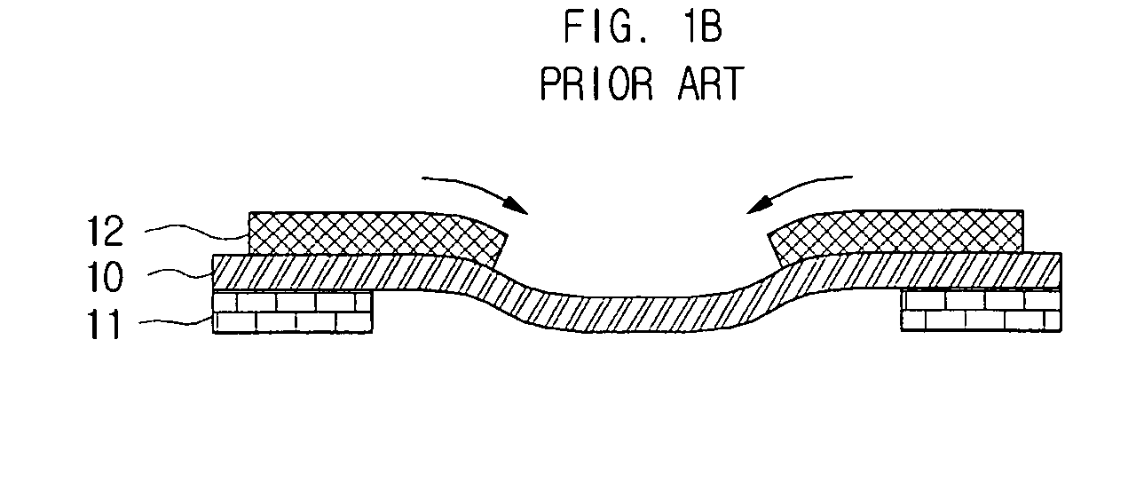
A MEMS component is generally made of multiple layers of thin film, and because of differences in the coefficients of thermal expansion between the thin films, is inevitably susceptible to problems of thermal deformation.
This thermal deformation in the component can be a major cause of changes in operational characteristics of the component, and if left unchecked, does not provide the intended operational characteristics, whereby the accuracy and reliability of the component are greatly degraded.
The problem of thermal deformation is especially serious in the bridge-cantilever type of thin film stack structure, such as that illustrated in FIG. 1.

Method used


Image

  • MEMS structure and optical modulator having temperature compensation layer
  • MEMS structure and optical modulator having temperature compensation layer
  • MEMS structure and optical modulator having temperature compensation layer

Examples


Embodiment Construction

[0039]As the present invention allows for various changes and numerous embodiments, particular embodiments will be illustrated in drawings and described in detail in the written description. However, this is not intended to limit the present invention to particular modes of practice, and it is to be appreciated that all changes, equivalents, and substitutes that do not depart from the spirit and technical scope of the present invention are encompassed in the present invention. In the description of the present invention, certain detailed explanations of related art are omitted when it is deemed that they may unnecessarily obscure the essence of the invention.

[0040]While such terms as “first” and “second,” etc., may be used to describe various elements, such elements must not be limited to the above terms. The above terms are used only to distinguish one element from another. For example, a first element may be referred to as a second element without departing from the scope of right...


PUM


Abstract

An optical modulator can be provided that includes a substrate; an insulation layer positioned on the substrate; a ribbon layer such that its center portion is spaced apart from the insulation layer; a piezoelectric actuator positioned on either end of the ribbon layer that provides the driving force which moves the center portion of the ribbon layer vertically; and a temperature compensation layer, which is made of a thermally contracting material having a negative coefficient of expansion, and which is formed on at least one position of an upper portion of the piezoelectric actuator, a lower portion of the piezoelectric actuator, and a lower surface of the ribbon layer corresponding to a position of the piezoelectric actuator. In the optical modulator, the problem of thermal deformation due to rises in temperature can be resolved, whereby the accuracy and reliability of operation of the component can be increased.

Description

CROSS-REFERENCE TO RELATED APPLICATION[0001]This application claims the benefit of Korean Patent Application No. 10-2007-0090975 filed with the Korean Intellectual Property Office on Sep. 7, 2007, the disclosure of which is incorporated herein by reference in its entirety.BACKGROUND[0002]1. Technical Field[0003]The present invention relates to a MEMS component, more particularly to a MEMS structure and optical modulator having a temperature compensation layer, to resolve the problem in a MEMS component including multiple thin film layers of thermal deformation caused by different coefficients of thermal expansion between thin films.[0004]2. Description of the Related Art[0005]MEMS refers to a microelectromechanical system or component, which is a technology that uses semiconductor manufacturing technology to form three-dimensional structures on silicon substrates. There are a variety of applications in which MEMS is used, an example of which is the field of optics. Using MEMS techno...

Claims


Application Information

Patent Timeline
IPC IPC(8): G02B26/00
CPCG02B26/0858G02B7/008Y10S359/904
Inventor WOO, KI-SUKSONG, JONG-HYEONGKIM, HEE-YEOUN
Owner SAMSUNG ELECTRO MECHANICS CO LTD
Learn More