
Silicon-Germanium Hydrides and Methods for Making and Using Same

a technology of silicongermanium hydride and silicongermanium hydride, which is applied in the field of silicongermanium alloys, silicongermanium alloys, semiconductor structures, can solve the problems of complex and fraught best current route to these materials, low growth rate of 0.2 nm/min, and inability to meet the requirements of high-throughput device fabrication

Inactive Publication Date: 2009-02-26
ARIZONA STATE UNIVERSITY
View PDF9 Cites 13 Cited by
  • Summary
  • Abstract
  • Description
  • Claims
  • Application Information

AI Technical Summary

Benefits of technology

[0013]In a second aspect, the present invention provides semiconductor structures, comprising a substrate and an Si—Ge layer formed by introducing near the surface of a substrate a gaseous precursor comprising one or more compounds according to formula I.
[0014]In further aspect, the invention provides semiconductor structures, comprising a substrate and an Si—Ge layer comprising a backbone of one or more compounds according to formula I.
[0015]In a third aspect, the present invention provides methods for synthesizing one or more silicon-germanium hydrides of formula I, comprising combining a compound selected from the group consisting of a nonafluorobutane-sulfonic substituted disilane and a triflate substituted disilane, with a compound comprising a ...

Problems solved by technology

Heteroepitaxial Ge1-xSix layers on Si(100) with high Ge contents are of interest due to many applications in key technologies such as solar cells, MEMS, quantum cascade lasers and Si-based photonics1,2 including high speed modulators and photodetectors.3 However, these materials are much less developed in spite of this high impact potential in IR optical devices.
In addition, they serve as virtual substrates for growth of high mobility, strained Si and Ge device channels, and are also considered as a potential pathway to monolithic integration of III-V based devices with Si technologies.4,5 The best current route to these materials is complicated and fraught with difficulties, requiring both high temperature growth of thick (>10 μm) compositionally graded films and a chemical-mechanical planarization step to relieve the misfit strain between the Ge1-xSix epilayer and Si substrate and produce a flat surface, respectively.6
However, in our experiments we have observed that stoichiometric Si0.50Ge0.50, with the required device quality properties (surface planarity, low defect densities), can only be grown near a maximum temperature of ˜450° C. at a growth rate of only 0.2 nm / min which is too low to be practical for high throughput device fabrication.

Method used


Image

  • Silicon-Germanium Hydrides and Methods for Making and Using Same
  • Silicon-Germanium Hydrides and Methods for Making and Using Same
  • Silicon-Germanium Hydrides and Methods for Making and Using Same

Examples


examples

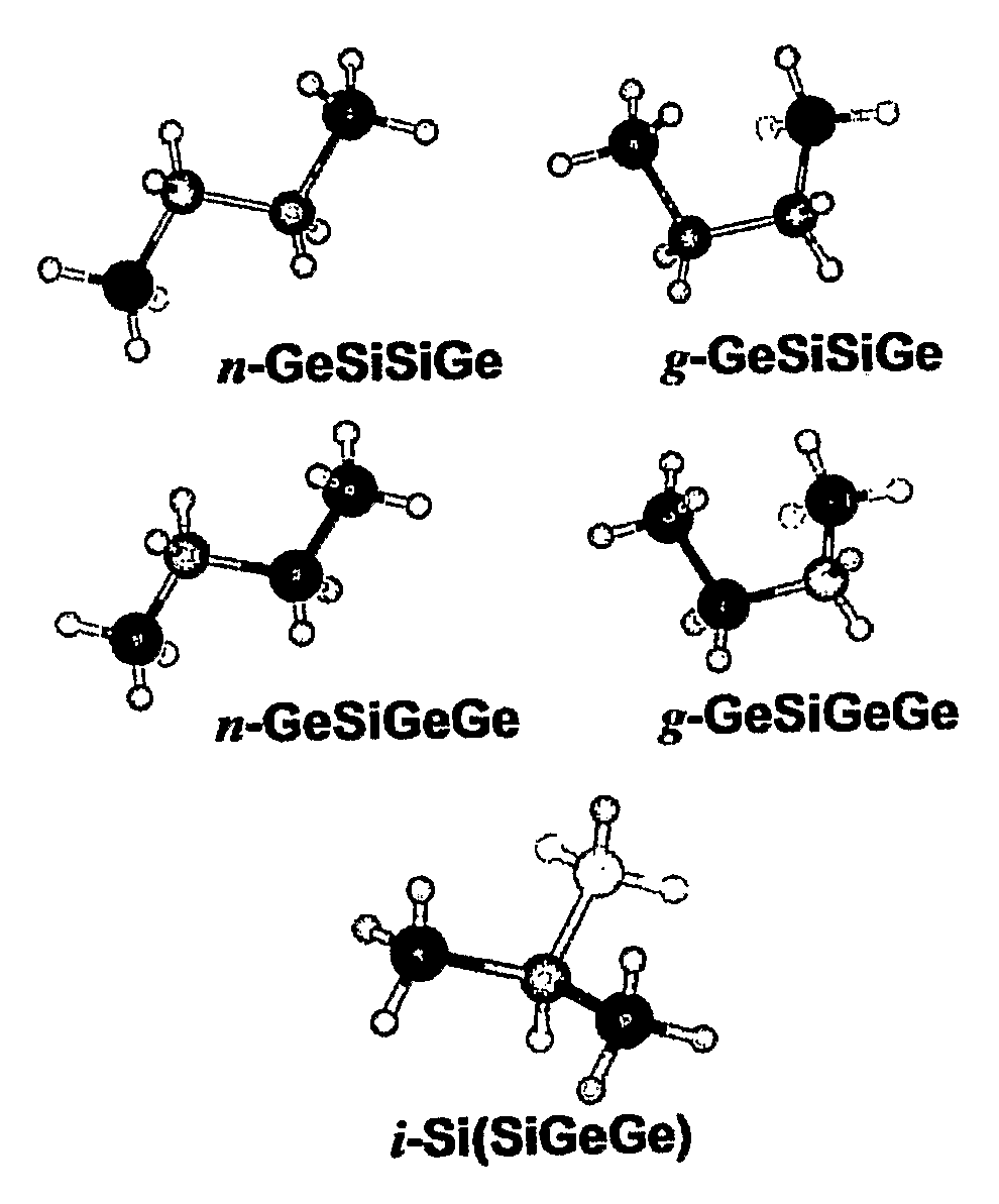
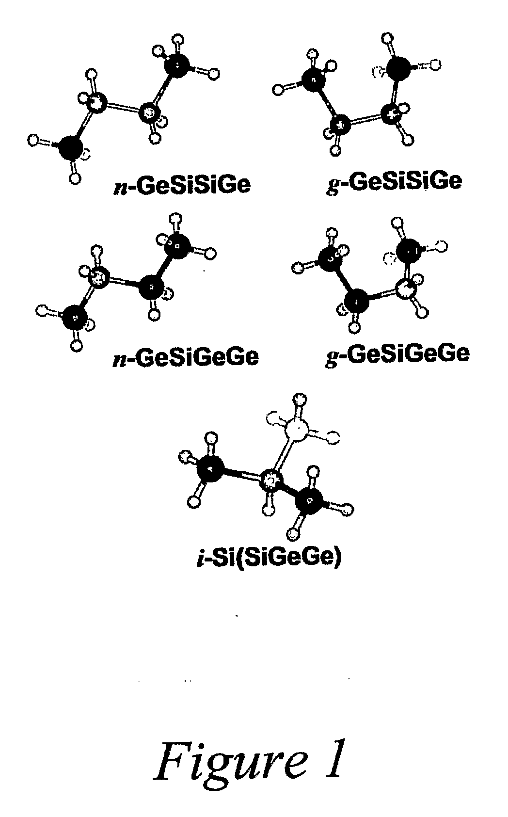
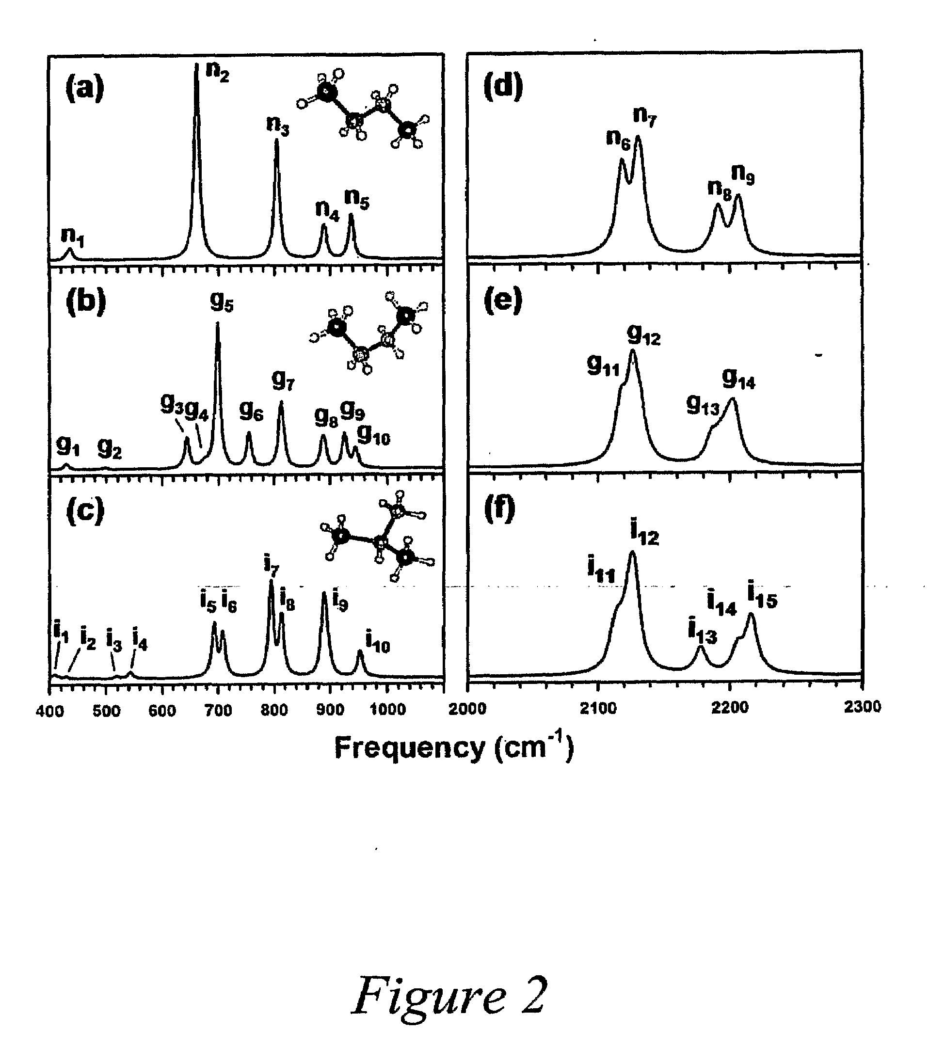
[0099]The synthesis of butane-like (GeH3)2(SiH2)2 (Also referred to as GeH3-SiH2-SiH2-GeH3) (1), (GeH3)2SiH(SiH3) (also referred to as SiH[(GeH3)2(SiH3)] (2) and (GeH3)2(SiH2GeH2) (referred to above as GeH3-SiH2-GeH2-GeH3) (3) Si—Ge hydrides with applications in low temperature synthesis of Ge-rich Si1-xGex optoelectronic alloys is herein demonstrated. The compositional, vibrational, structural and thermochemical properties of these compounds were studied by FTIR, multinuclear NMR, mass spectrometry, Rutherford backscattering, and density functional theory (DFT) simulations. The analyses indicate that the linear (GeH3)2(SiH2)2 (1) and (GeH3)2(SiH2GeH2) (3) compounds exist as a mixture of the classic normal and gauche conformational isomers which do not seem to interconvert at 22° C. The conformational proportions in the samples were determined using a new fitting procedure, which combines calculated molecular spectra to reproduce those observed by varying the global intensity, frequ...


PUM

PropertyMeasurementUnit
Temperatureaaaaaaaaaa
Thicknessaaaaaaaaaa

Abstract

The present invention provides silicon-germanium hydride compounds, methods for their synthesis, methods for their deposition, and semiconductor structures made using the compounds. The compounds are defined by formula: SiHnI (GeHn2)y, wherein y is 2, 3, or 4 wherein n1 is 0 1, 2 or 3 to satisfy valency and wherein n2 is independently 0, 1, 2 or 3 for each Ge atom in the compound, to satisfy valency.

Description

CROSS REFERENCE TO RELATED APPLICATIONS[0001]This application claims the benefit of U.S. Provisional Patent Application Ser. Nos. 60 / 739,528 filed Nov. 23, 2005 and 60 / 64,063 filed Feb. 1, 2006, both of which are incorporated by reference herein in their entirety.STATEMENT OF GOVERNMENT INTEREST[0002]This work was supported by National Science Foundation grant DMR-0221993 thus the U.S. government may have certain rights in the invention.FIELD OF THE INVENTION[0003]The present application relates generally to the fields of chemistry, optoelectronics, silicon-germanium alloys, semiconductor structures, and related methods and devices.BACKGROUND[0004]Heteroepitaxial Ge1-xSix layers on Si(100) with high Ge contents are of interest due to many applications in key technologies such as solar cells, MEMS, quantum cascade lasers and Si-based photonics1,2 including high speed modulators and photodetectors.3 However, these materials are much less developed in spite of this high impact potentia...

Claims


Application Information

Patent Timeline
IPC IPC(8): H01L29/24C01B33/04B32B9/04C30B23/02H01B1/06H01B1/04H01B1/02
CPCC01B6/06C23C16/22C30B25/02C30B29/52Y10T428/265H01L21/02381H01L21/02532H01L21/0262Y10T428/261H01L21/0237Y10T428/31663C07F7/02
Inventor KOUVETAKIS, JOHNRITTER III, COLE J.
Owner ARIZONA STATE UNIVERSITY
Learn More