Electronic Assemblies Without Solder Having Overlapping Components

a technology of electronic components and soldering, which is applied in the direction of printed circuit non-printed electric components association, sustainable manufacturing/processing, and final product manufacturing, etc. it can solve the problems of tin and lead, serious chemical disadvantages of soldering materials, and potentially damaging human health and the environment, so as to improve the density of electrical components, reduce the number of layers, and increase the routing channel

Active Publication Date: 2009-02-05
FJELSTAD JOSEPH CHARLES
View PDF13 Cites 0 Cited by
  • Summary
  • Abstract
  • Description
  • Claims
  • Application Information

AI Technical Summary

Benefits of technology

[0014]To improve the density of electrical components in a circuit assembly, components can be overlapped. In addition, the components can be encapsulated in an electronic insulating material. This assembly offers significant design benefits in solderless assembly including an increase in routing channels, a reduction in layer count, and an elimination of solder shorts and opens however, as previously stated they can be used as components either integrated or simply bonded to one another to create a stacked assembly without encapsulation, again however, lead frame components would potentially be subject to bending out of alignment.

Problems solved by technology

One set of disadvantages relates to solder materials themselves.
Unfortunately, both tin and especially lead have serious chemical disadvantages.
For these two metals, mining the ores, refining it, working with the refined metals during manufacturing, being exposed to the substances in manufactured products, and disposing of the products at the ends of their life cycles are all potentially damaging to human health and to the environment.
Mining, refining, working during manufacturing, exposure from manufactured products, and disposal are still all issues for tin, silver, and copper.
It therefore suffices here to say that the undue use of some materials, like solder, is generally undesirable in electronic assemblies.
Another set of disadvantages in the solder-based assembly of electronic products is the heat-based processes that are inherently required.
The use of heat on and around many electronic components has always been undesirable.
As a general principle, the heating of electronic components increases their failure rate and beyond a certain point outright damages such components.
This is not as frequently the same for SAC type solders, however, which melt at much higher temperatures.
When SAC type solders are used, the likelihood of component damage is much higher, resulting in assemblies that fail during post-manufacturing testing as well as in-the-field failures.
Additionally, generating and managing the heat during manufacturing have energy, safety, and financial costs.
In addition, the undue use of lead-based manufacturing processes, like soldering, is also generally undesirable in electronic assemblies.
Increasingly yet another set of disadvantages in the solder-based assembly of electronic products is related to the “adding” of materials.
When a material, like solder, is added between two components to hold them together, the additional material inherently has to occupy some space.
The use of liquid-state materials, like solder in its liquid stage, in manufacturing often requires additional space around leads, terminals, and pads because both product and process designs need to account for the ability of liquid to flow easily and thus to potentially short to other leads, terminals, pads, etc.
So the undue use of additional material, including solder, in manufactured assemblies and manufacturing processes is generally undesirable.

Method used


Image

  • Electronic Assemblies Without Solder Having Overlapping Components
  • Electronic Assemblies Without Solder Having Overlapping Components
  • Electronic Assemblies Without Solder Having Overlapping Components

Examples


Embodiment Construction

[0028]The foregoing description details specific embodiments of the invention and are included for illustrative purposes. However, it will be apparent to one skilled in the art that many combinations and permutations of the following embodiments are possible while remaining within the scope and spirit of the invention.

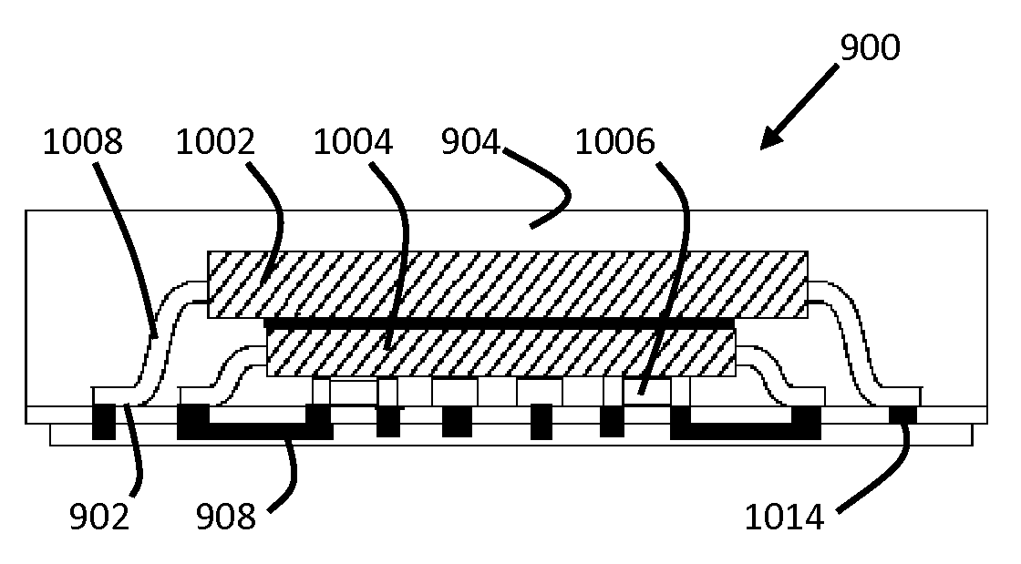
[0029]FIG. 1 shows a subassembly 100 viewed from the lead termination (also referred to “pad” or “land” in the art) side of components encapsulated in electrical / electronic insulating material 104. Exposed are terminations such as gull wing component lead termination 102 and discrete or analog component lead termination 106.

[0030]FIG. 2 is a section taken along 2-2 of FIG. 1 of subassembly 100. Shown previously in FIG. 1, the relative positions of electronic insulating material 104, exposed terminations, such as gull wing component lead termination 102 and discrete or analog component lead termination 106, are shown in FIG. 2. Upper gull wing component package 202, hav...


PUM


Abstract

An apparatus is disclosed that improves density of electrical components in a circuit assembly. Electrical components 202, 204 are stacked so that they overlap each other and are encapsulated in an electronic insulating material 104. The resulting subassembly may be integrated onto a printed circuit board or into a reverse-interconnection process assembly.

Description

CROSS-REFERENCE TO RELATED APPLICATIONS[0001]This application claims the benefit of U.S. Provisional Application No. 60 / 962,627, filed on Jul. 31, 2007, hereby incorporated by reference in its entirety; U.S. Provisional Application No. 60 / 963,822, filed on Aug. 6, 2007, hereby incorporated by reference in its entirety; U.S. Provisional Application No. 60 / 966,643, filed on Aug. 28, 2007, hereby incorporated by reference in its entirety; U.S. Provisional Application No. 61 / 038,564, filed on Mar. 21, 2008, hereby incorporated by reference in its entirety; U.S. Provisional Application No. 61 / 039,059 filed on Mar. 24, 2008, hereby incorporated by reference in its entirety; and U.S. Provisional Application No. 61 / 075,238 filed on Jun. 24, 2008, hereby incorporated by reference in its entirety.[0002]This application is a continuation-in-part application of pending U.S. patent application Ser. No. 12 / 119,287, ELECTRONIC ASSEMBLIES WITHOUT SOLDER AND METHODS FOR THEIR MANUFACTURE; U.S. paten...

Claims


Application Information

Patent Timeline
IPC IPC(8): H05K1/18H05K7/02
CPCH01L25/105H01L2924/14H01L2924/0002H01L2924/3025H01L2225/1005H05K1/023H05K1/185H05K3/284H05K3/4664H05K2201/10515H05K2201/10628H05K2201/10636H05K2201/10689H05K2201/10704H05K2201/10719H05K2201/10734H05K2203/1469H01L25/16H01L2225/1029H01L2225/107H01L2924/00H01L2924/15311H01L2924/15312H01L2924/15313Y02P70/50
Inventor GAMINI, NADERFJELSTAD, JOSEPH C.
Owner FJELSTAD JOSEPH CHARLES
Why Eureka
Try Eureka