
Apparatus and method for removing organic contamination adsorbed onto substrate, and apparatus and method for measuring thickness of thin film formed on substrate

a technology of organic contamination and substrate, which is applied in the direction of lighting and heating apparatus, semiconductor/solid-state device testing/measurement, and instruments. it can solve the problems of deterioration of the film formed on the substrate, inability to efficiently perform required processes, and difficulty in completely eliminating the foregoing solutions. it can reduce the re-adsorption of organic contamination, facilitate the movement of the substrate, and simplify the structure of the apparatus.

Inactive Publication Date: 2009-01-22
DAINIPPON SCREEN MTG CO LTD
View PDF7 Cites 9 Cited by
  • Summary
  • Abstract
  • Description
  • Claims
  • Application Information

AI Technical Summary

Benefits of technology

The present invention is about an apparatus for removing organic contamination from a substrate and preventing it from re-adsorbing back onto the substrate. The apparatus includes a hot plate for heating the substrate, a cooling plate for cooling the substrate, a transfer mechanism for moving the substrate from the hot plate to the cooling plate, and a chamber body where the substrate passes through during the transfer process. The apparatus also includes a film-thickness measuring part, such as an ellipsometer, for accurately measuring the thickness of a thin film on the substrate after organic contamination is removed. The invention provides a simple and effective way to remove organic contamination and measure the thickness of thin films on substrates.

Problems solved by technology

It is additionally noted that though to employ a material which releases little gas as a substrate container for storing a substrate, or to provide a chemical filter, might be of some help to suppression of adsorption of organic contamination onto the substrate, it is difficult to completely eliminate released gas by the foregoing solutions.
However, this method has the possibility of deteriorating a film formed on a substrate.
Hence, required processes cannot be efficiently performed.
This increases the possibility that organic contamination will be again adsorbed onto the substrate.

Method used


Image

  • Apparatus and method for removing organic contamination adsorbed onto substrate, and apparatus and method for measuring thickness of thin film formed on substrate
  • Apparatus and method for removing organic contamination adsorbed onto substrate, and apparatus and method for measuring thickness of thin film formed on substrate
  • Apparatus and method for removing organic contamination adsorbed onto substrate, and apparatus and method for measuring thickness of thin film formed on substrate

Examples


Embodiment Construction

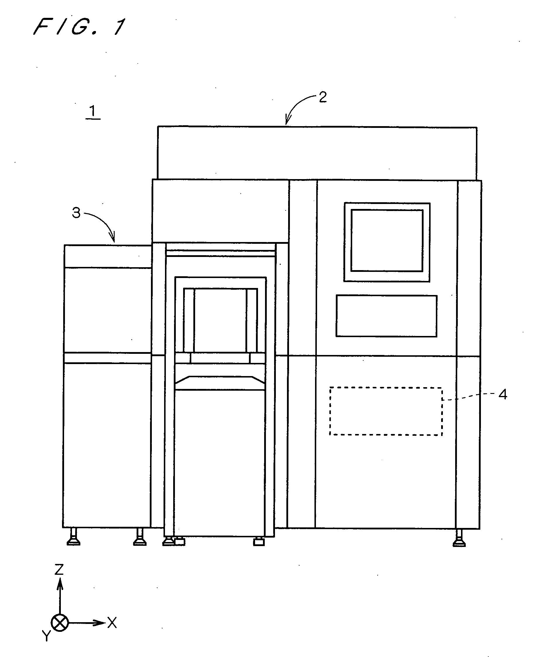
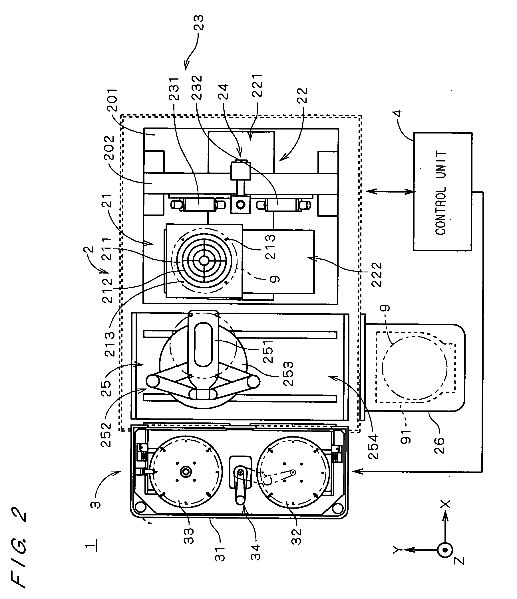
[0028]FIG. 1 is a front view of a film-thickness measuring apparatus 1 according to a first preferred embodiment of the present invention. As illustrated in FIG. 1, a body 2 of the film-thickness measuring apparatus 1 is provided with an organic contamination remover 3 for removing (or desorbing) organic contamination adsorbed onto (or adhering to) a substrate. Also, a control unit 4 allocated to overall control of the film-thickness measuring apparatus 1 is provided under the body 2. In the film-thickness measuring apparatus 1, a thickness of a thin film (or thin films) (an oxide film, for example) formed on a substrate is measured by constituent elements in the body 2 after organic contamination adsorbed onto the substrate is removed by the organic contamination remover 3. Below, the body 2 and the organic contamination remover 3 will be described in detail.

[0029]FIG. 2 illustrates an internal structure of the film-thickness measuring apparatus 1. It is noted that hatching lines f...


PUM


Abstract

In a body of a film-thickness measuring apparatus (1), an organic contamination remover (3) for removing organic contamination adsorbed onto a substrate (9) is provided. The organic contamination remover (3) includes a chamber body (31), an interior of which is kept clean. In the chamber body (31), a hot plate (32) for heating the substrate, a cooling plate (33) for cooling the substrate, and a transfer arm (34) for moving the substrate (9) from the hot plate (32) to the cooling plate (33) in the chamber body 31, are provided. With this structure, it is possible to keep the substrate (9) in a clean atmosphere within the chamber body (31), to thereby suppress re-adsorption of organic contamination onto the substrate during a time period from a time when organic contamination adsorbed onto the substrate (9) is removed to a time when cooling is completed.

Description

BACKGROUND OF THE INVENTION[0001]1. Field of the Invention[0002]The present invention relates to an apparatus and a method for removing organic contamination adsorbed onto a substrate, and more particularly to a technique for measuring a thickness of a thin film formed on a substrate.[0003]2. Description of the Background Art[0004]In recent years, as a circuit pattern of a semiconductor product has become finer based on a scaling law, a thickness of a film formed on a semiconductor substrate (which will hereinafter be referred to as a “substrate”) in semiconductor manufacturing processes has become smaller. It is expected that a film thickness of silicon oxide (SiO2) serving as a gate insulator is equal to or smaller than 1 nm for 65-nm technology node (i.e., a node length), for example, in the future.[0005]On the other hand, it is well known that an optical measurement value of a film thickness is increased due to exposure of a substrate to an atmospheric air in a clean room or sto...

Claims


Application Information

Patent Timeline
Patent Type & Authority Applications(United States)
IPC IPC(8): F26B7/00F26B19/00G01B11/06H01L21/00H01L21/66
CPCB08B7/0071B08B9/00H01L21/67253H01L21/67069H01L21/67103G01B11/0641B24B3/44B24B41/06B24B55/03
Inventor NAKAZAWA, YOSHIYUKIKONO, MOTOHIROKITAJIMA, TOSHIKAZUISO, DAISUKE
Owner DAINIPPON SCREEN MTG CO LTD
Learn More