Semiconductor device and method for manufacturing the same

a technology of semiconductor devices and dielectric layers, applied in the direction of semiconductor devices, basic electric elements, electrical equipment, etc., can solve the problems of reducing the efficiency of the gate insulation layer, the inability to conduct the leakage current caused by the direct tunnel current, and the state threshold voltage, etc., to suppress the formation of low dielectric layers, suppress the threshold voltage shift, and suppress the reaction

Inactive Publication Date: 2008-12-25
TOSHIBA MEMORY CORP
View PDF12 Cites 0 Cited by
  • Summary
  • Abstract
  • Description
  • Claims
  • Application Information

AI Technical Summary

Benefits of technology

[0012]The present invention has been achieved in order to solve the problems. An object of the present invention is to provide a semiconductor device, and its manufacturing method, capable of suppressing reaction between the insulation layer component and silicon, suppressing formation of the low dielectric layer on the surface of the insulation layer, and suppressing the threshold voltage shift in a high dielectric constant insulation layer applied to semiconductor devices.
[0020]According to the present embodiments, it is possible to provide a semiconductor device, and its manufacturing method, capable of suppressing reaction between the insulation layer component and silicon, suppressing formation of the low dielectric layer on the surface of the insulation layer, and suppressing the threshold voltage shift in a high dielectric constant insulation layer applied to semiconductor devices.

Problems solved by technology

In this film thickness region, however, suppression of leakage current caused due to a direct tunnel current cannot be conducted, and SiO2 can no longer be used as a gate insulation layer because of a resultant increase of power dissipation.
There is not only the problem of presence of the low dielectric constant interface, but also a problem that a ON state threshold voltage at which an MISFET with such a gate insulation layer shifts from its ideal value.
This results in a problem that the on-current cannot be ensured in a low power supply voltage state.
These problems of the formation of the low dielectric constant layer and the threshold shift occur not only in the gate insulation layer using the Hf material, but also in a high dielectric constant gate insulation layer using an oxide of Zr, Ti or Ta, which is metal in which silicon in the substrate can be diffused, or metal which can react with polycrystalline silicon serving as the electrode, in the same way.

Method used


Image

  • Semiconductor device and method for manufacturing the same
  • Semiconductor device and method for manufacturing the same
  • Semiconductor device and method for manufacturing the same

Examples


Embodiment Construction

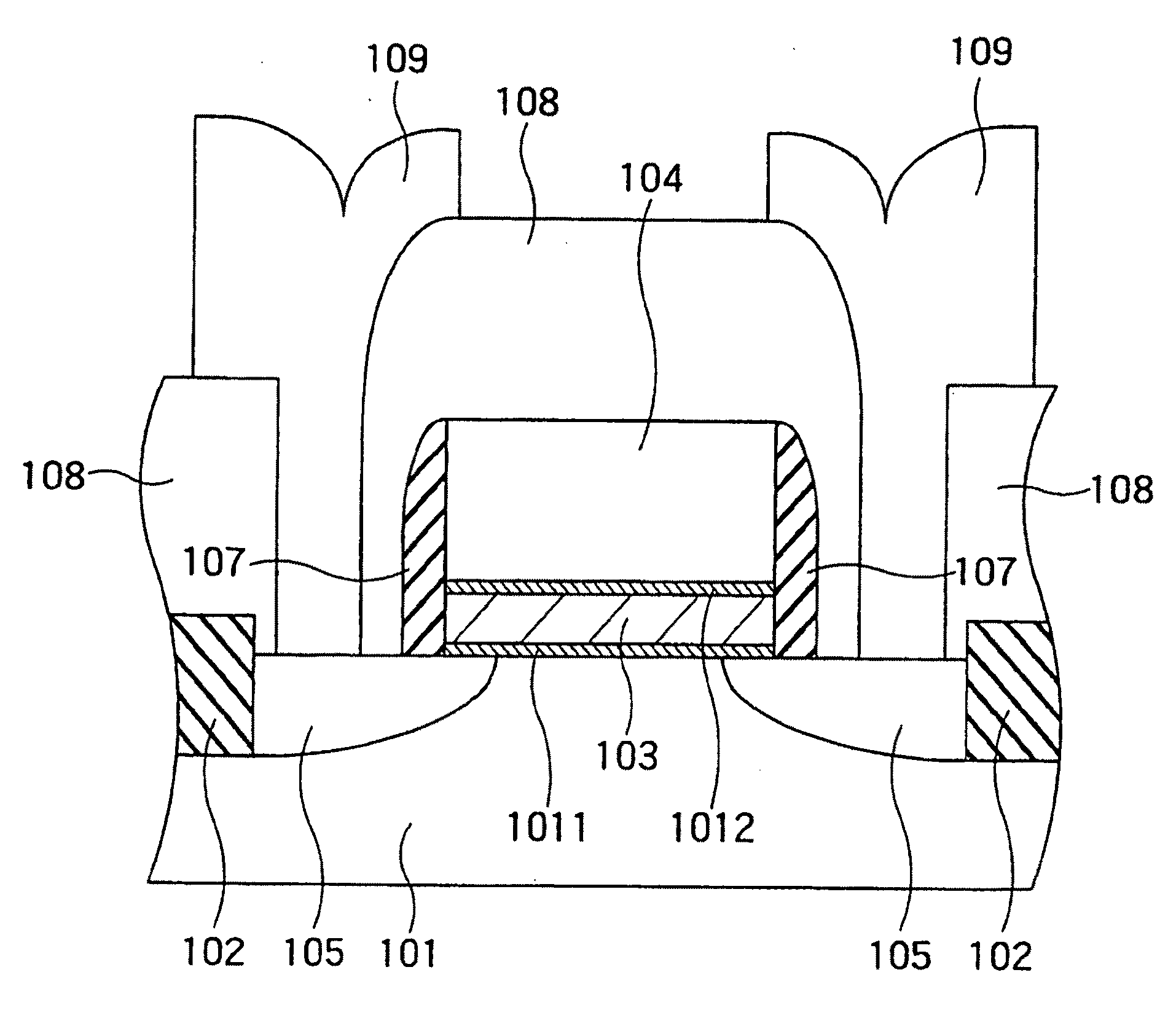
[0029]The present inventors have studied energetically in order to solve the problems. Paying attention to the fact that the every problem is caused by reaction conducted between an element forming the insulation layer and silicon forming the silicon substrate or electrode, the present inventors have found that a structure having a barrier layer formed of a material that suppresses the interface reaction at upper and lower interfaces and diffusion of silicon from the substrate is effective. In other words, the present invention provides a structure having, as the barrier layer at at least the upper or lower interface of the high dielectric constant insulation layer, an insulation layer having a dielectric constant that is sufficiently high as compared with SiO2 without causing the silicon diffusion and the silicide formation reaction with silicon, and / or formation of a low dielectric constant interface layer.

[0030]Hereafter, the present invention will be described in detail.

[0031]Fi...


PUM

PropertyMeasurementUnit
thicknessaaaaaaaaaa
thicknessaaaaaaaaaa
sizeaaaaaaaaaa

Abstract

A semiconductor device includes a silicon substrate; an insulation layer formed on the silicon substrate, the insulation layer containing an oxide of an element of at least one kind selected from at least Hf, Zr, Ti and Ta; an electrode formed on the insulation layer; and a metal oxide layer containing La and Al, the metal oxide layer being provided at at least one of an interface between the silicon substrate and the insulation layer and an interface between the insulation layer and the electrode.

Description

CROSS-REFERENCE TO RELATED APPLICATIONS[0001]This application is based upon and claims the benefit of priority from the prior Japanese Patent Applications No. 2004-264828, filed on Sep. 13, 2004, the entire contents of which are incorporated herein by reference.BACKGROUND OF THE INVENTION[0002]1. Field of the Invention[0003]The present invention relates to a semiconductor device and its manufacturing method. In particular, the present invention relates to a semiconductor device that includes an insulation layer having a high dielectric constant and its manufacturing method.[0004]2. Background Art[0005]The scale down of CMOS LSIs demand thinner gate insulation layers. Gate insulation layers in the next generation MOS field effect transistors having a size smaller than 0.1 μm are demanded to have equivalent oxide thickness of 1.5 nm or less. In this film thickness region, however, suppression of leakage current caused due to a direct tunnel current cannot be conducted, and SiO2 can no...

Claims


Application Information

Patent Timeline
Patent Type & Authority Applications(United States)
IPC IPC(8): H01L21/28
CPCH01L21/2807H01L21/28194H01L29/495H01L29/4966H01L29/4975H01L29/513H01L29/517H01L29/516
Inventor SUZUKI, MASAMICHIMATSUSHITA, DAISUKEYAMAGUCHI, TAKESHI
Owner TOSHIBA MEMORY CORP
Why Eureka
Try Eureka