
Integrated Circuit Amplifiers Having Switch Circuits Therein that Provide Reduced 1/f Noise

a technology of integrated circuits and switch circuits, which is applied in the direction of differential amplifiers, amplifier modifications to reduce noise influence, pulse automatic control, etc., can solve the problem of further degrading the 1/f noise characteristics of cmos circuits, further worsening the signal-to-noise ratio (snr) of cmos communication semiconductor circuits, and 1/f noise may become the main noise source of up to several hundreds of kh through several tens

Inactive Publication Date: 2008-12-25
SAMSUNG ELECTRONICS CO LTD
View PDF6 Cites 20 Cited by
  • Summary
  • Abstract
  • Description
  • Claims
  • Application Information

AI Technical Summary

Benefits of technology

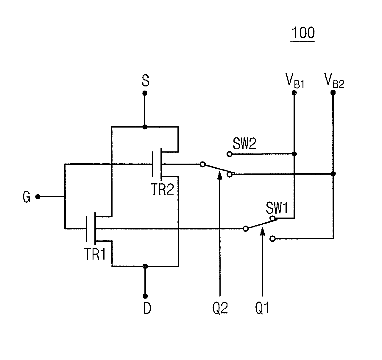
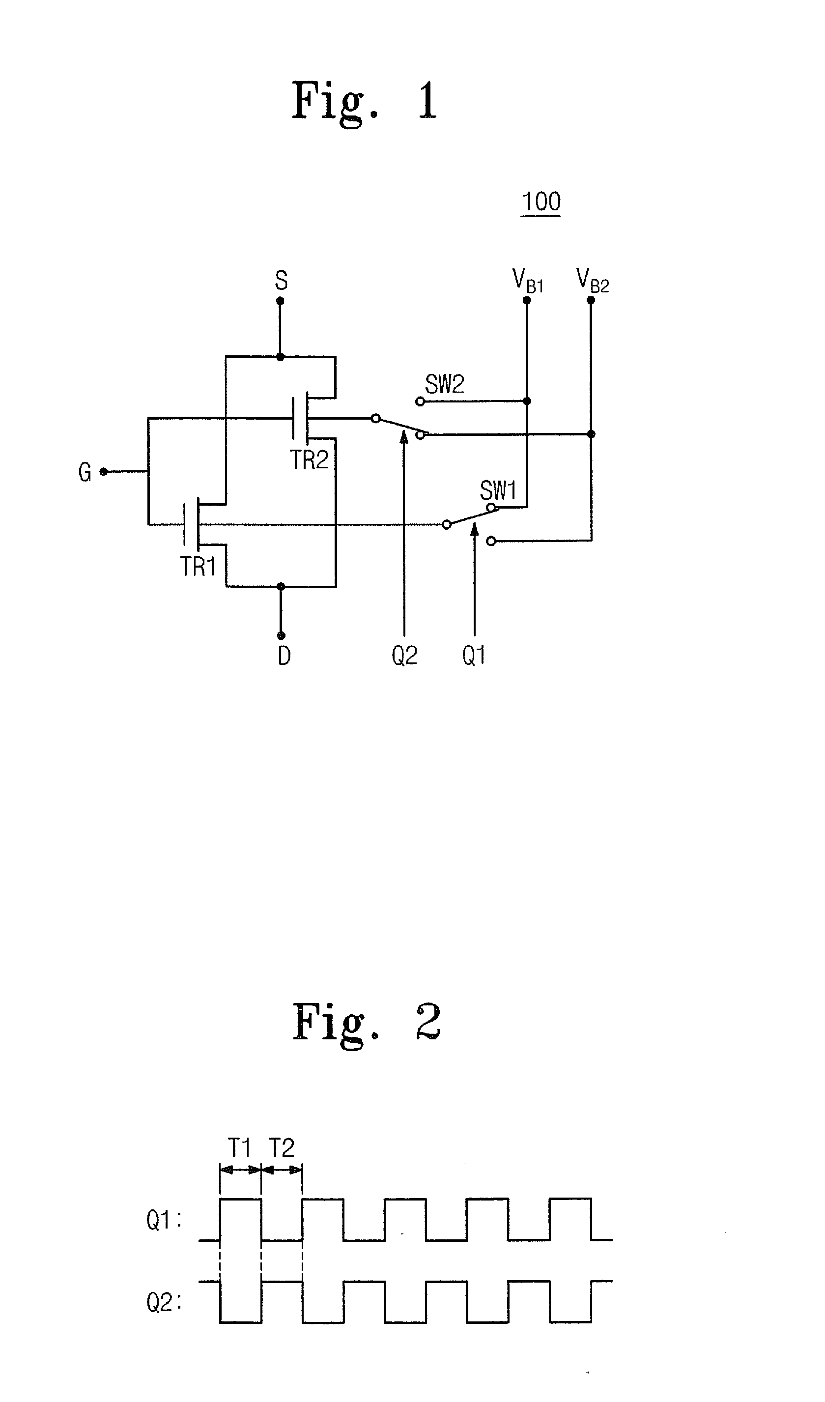
[0004]Integrated circuit devices according to some embodiments of the present invention include a pair of field effect transistors having shared source terminals, shared drain terminals and shared gate terminals, which may be treated herein as being electrically coupled in parallel. A switch circuit is also provided. The switch circuit is configured to drive a body terminal of a first one of the pair of field effect transistors with an alternating sequence of first and second unequal body voltages. This alternating sequence is synchronized with a first clock signal. T...

Problems solved by technology

Also, the down-scaling of CMOS circuits may further degrade the 1 / f noise characteristics of CMOS circuits.
However, the degradation of the 1 / f noise characteristics of CMOS circuits further worsens a signal-to-noise ratio (SNR) of CMOS communication semiconductor circuits.
If a CMOS direct conversion receiver is implemented in a narrowband communication system, such as the Global System for Mobile Communications (GSM), the 1 / f noise may become the main noise source of up to several hundreds of kH through several tens of MHz.

Method used


Image

  • Integrated Circuit Amplifiers Having Switch Circuits Therein that Provide Reduced 1/f Noise
  • Integrated Circuit Amplifiers Having Switch Circuits Therein that Provide Reduced 1/f Noise
  • Integrated Circuit Amplifiers Having Switch Circuits Therein that Provide Reduced 1/f Noise

Examples


Embodiment Construction

[0015]Preferred embodiments of the present invention will be described below in more detail with reference to the accompanying drawings. The present invention may, however, be embodied in different forms and should not be construed as limited to the embodiments set forth herein. Rather, these embodiments are provided so that this disclosure will be thorough and complete, and will fully convey the scope of the present invention to those skilled in the art.

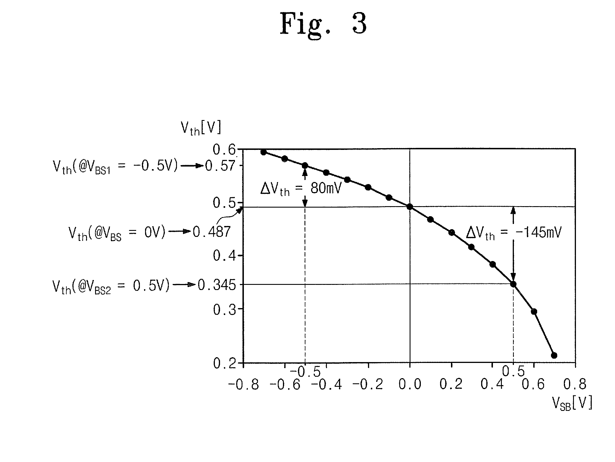
[0016]A complementary metal oxide semiconductor (CMOS) amplifier according to the present invention can reduce 1 / f noise (i.e., a low-frequency noise) by using two field-effect transistors (FETs) connected in parallel. The CMOS amplifier according to the present invention includes: a first transistor including a first source, a first gate, a first drain, and a first body; a second transistor including a second source, a second gate, a second drain, and a second body; a source terminal connecting the first source and the second sourc...


PUM


Abstract

Integrated circuit devices include a pair of field effect transistors having shared source terminals, shared drain terminals and shared gate terminals, which may be treated herein as being electrically coupled in parallel. A switch circuit is also provided, which is configured to drive a body terminal of a first one of the pair of field effect transistors with an alternating sequence of first and second unequal body voltages. This alternating sequence is synchronized with a first clock signal. The switch circuit is also configured to drive a body terminal of a second one of the pair of field effect transistors with an alternating sequence of third and fourth unequal body voltages, which is synchronized with a second clock signal. The first and third body voltages may have equivalent magnitudes and the second and fourth body voltages may have equivalent magnitudes. The first and second clock signals may have 50% duty cycles and may be 180 degrees out-of-phase relative to each other.

Description

REFERENCE TO PRIORITY APPLICATION[0001]This U.S. non-provisional patent application claims priority under 35 U.S.C. § 119 to Korean Patent Application No. 10-2007-0090613, filed Sep. 6, 2007, the entire contents of which are hereby incorporated herein by reference.FIELD OF THE INVENTION[0002]The present invention relates to integrated circuit devices and, more particularly, to integrated circuit amplifiers and methods of operating same.BACKGROUND OF THE INVENTION[0003]In comparison with bipolar or GaAs semiconductor circuits, radio frequency (RF) CMOS circuits may have high 1 / f noise (i.e., a low-frequency noise), which is dominant in the frequency domain unlike thermal noise. Also, the down-scaling of CMOS circuits may further degrade the 1 / f noise characteristics of CMOS circuits. The down-scaling of CMOS circuits reduces a supply voltage and is advantageous in terms of power amplification. However, the degradation of the 1 / f noise characteristics of CMOS circuits further worsens ...

Claims


Application Information

Patent Timeline
IPC IPC(8): H03F3/45H03L7/00
CPCH03F1/26H03F3/45179H03F2200/366H03F2200/372H03F2203/45342H03F2203/45371H03F2203/45396H03F3/45
Inventor KOH, JEONGWOOKSUH, CHUN-DEOKPARK, EUN-CHUL
Owner SAMSUNG ELECTRONICS CO LTD
Learn More