
Non-volatile semiconductor memory device

a semiconductor memory and non-volatile technology, applied in semiconductor devices, instruments, electrical appliances, etc., can solve the problems of large erase current, large area of memory modules, and insufficient reduction of the threshold voltage of memory transistors after erase, and achieve the effect of small erase curren

Inactive Publication Date: 2008-10-23
RENESAS ELECTRONICS CORP
View PDF10 Cites 7 Cited by
  • Summary
  • Abstract
  • Description
  • Claims
  • Application Information

AI Technical Summary

Benefits of technology

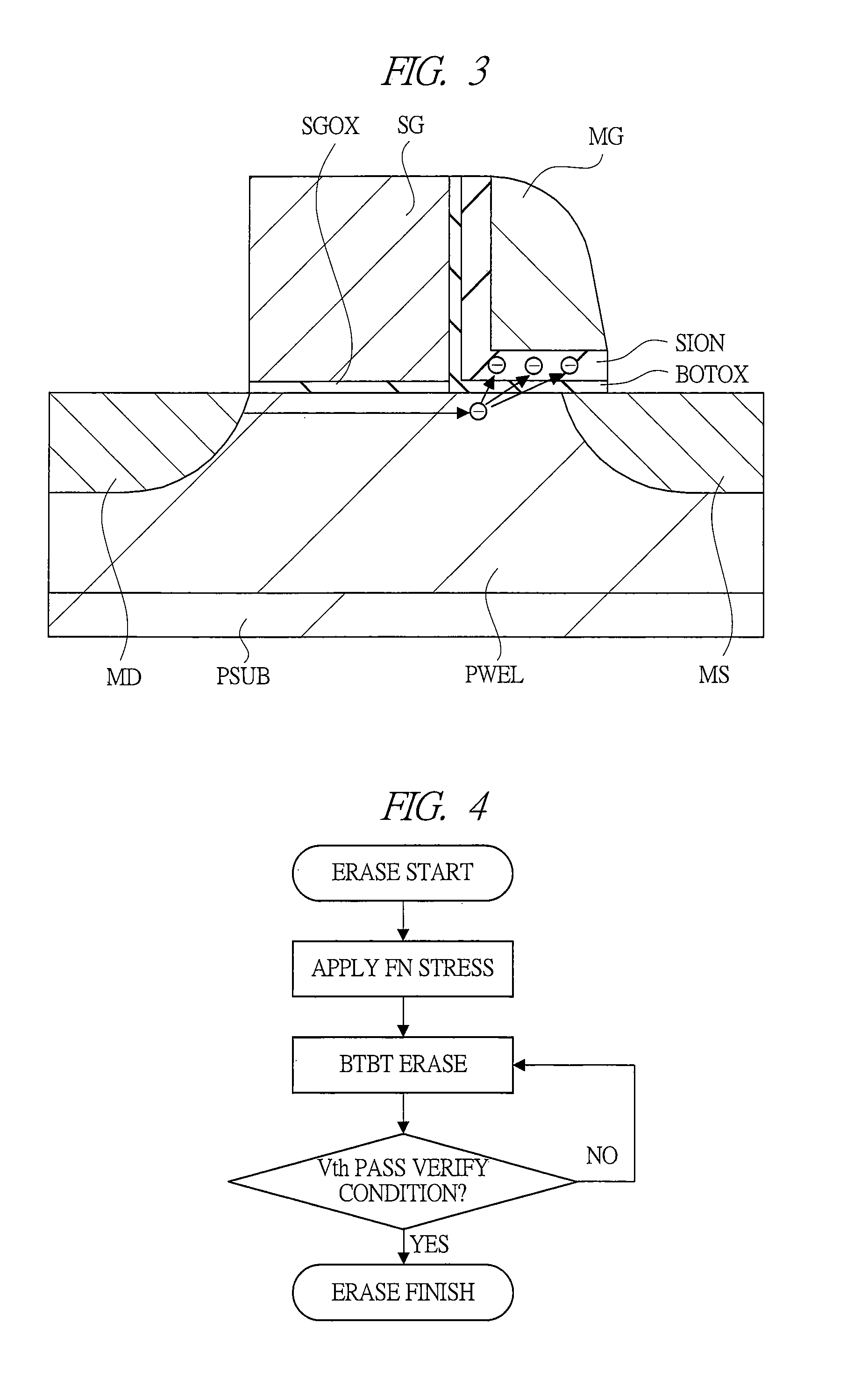
[0009]Therefore, as another one of the erase methods of the MONOS-type transistor, there is a method of injecting hot holes generated by the band-to-band tunneling phenomenon into the charge accumulation film. Specifically, by applying a positive voltage to the source region MS and applying a negative voltage to the memory gate electrode MG, holes are generated at an end of the source region MS by the band-to-band tunneling phenomenon. Then, the generated holes are accelerated by an electric field generated by high voltages applied to the source region MS and the memory gate electrode MG to be hot holes, and the generated hot holes are injected into the charge-trapping 5 silicon nitride film SIN, so that the erase operation is performed (see FIG. 34). According to this BTBT erase method, since hot holes are injected into the charge trapping film, the charge trapping film can be made to transit to a positive-charge accumulation state passing through a charge neutral state. Therefore, the threshold voltage of the memory transistor can be sufficiently decreased, a large read current can be obtained, and therefore, this method is suitable for high-speed operation.
[0011]An object of the present invention is to provide a technique capable of decreasing the erase current while keeping the advantages of the BTBT erase method.
[0016]By decreasing the erase current of the non-volatile semiconductor memory device, an occupied area of the charge pumping circuit can be decreased and the area of the memory module can be decreased. In other words, by reducing the erase current of the non-volatile semiconductor memory device, the number of cells erased at the same time can be increased and the erase time can be decreased.

Problems solved by technology

This erase method utilizing a tunneling phenomenon has an advantage that an erase current is small, and on the other hand, has a problem that the threshold voltage of the memory transistor cannot be sufficiently decreased after erase.
However, in the BTBT erase method, there is a problem that the erase current becomes large.
If the erase current is large, a charge pumping circuit with a large area for supplying a current is required, and as a result, an area of a memory module becomes large.
And, if the erase current is large, there are problems that the number of memory cells erased at the same time is restricted and an erase time for the entire erase block becomes long.

Method used


Image

  • Non-volatile semiconductor memory device
  • Non-volatile semiconductor memory device
  • Non-volatile semiconductor memory device

Examples


first embodiment

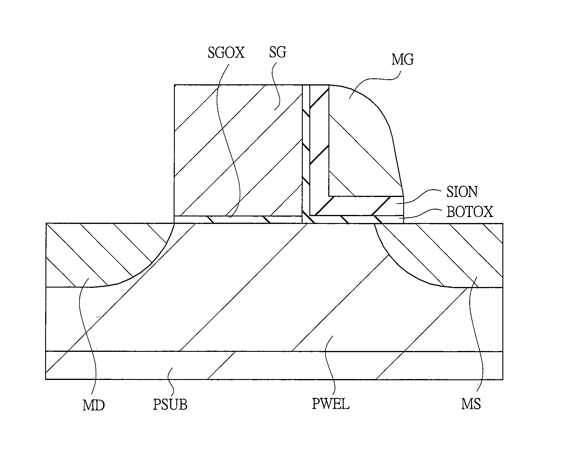
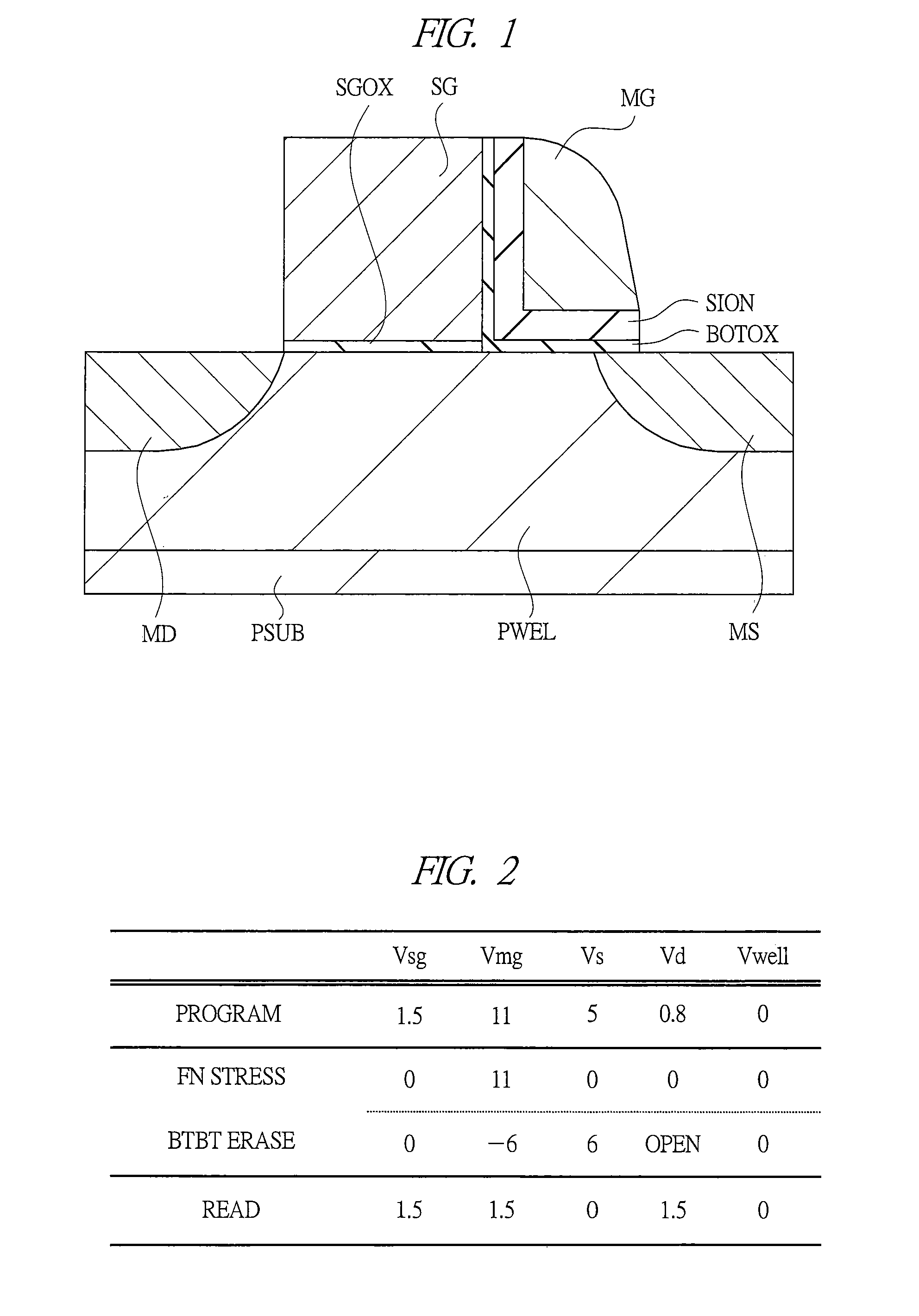
[0057]FIG. 1 is a cross-sectional view of main portions of a memory cell configuring a representative non-volatile semiconductor memory device (flash memory) according to a first embodiment. The memory cell shown here is a split-gate-type cell using a charge-trapping dielectric film. The charge-trapping dielectric film is a dielectric film having a discrete trap level therein and having a function of accumulating a charge at this trap level.

[0058]In the side of the surfaces of semiconductor substrate in the p-type well PWEL, a source region MS and a drain region MD are formed. Between the source region MS and the drain region MD, a select gate electrode SG is formed on a gate dielectric film SGOX to form a select transistor. On the other hand, over one side wall of the select gate electrode SG, a memory gate electrode MG is formed on a bottom silicon oxide film BOTOX, a silicon nitride film SIN and a top silicon oxide film TOPOX to form a memory transistor. The MONOS-type transistor...

second embodiment

[0142]FIG. 27 is a cross-sectional view of main portions of a representative non-volatile semiconductor memory device (memory cell) according to a second embodiment. A memory cell of the non-volatile semiconductor memory device shown here is a single-gate-type cell using a charge-trapping dielectric film as the charge accumulation film.

[0143]As shown in FIG. 27, the memory cell comprises the silicon oxynitride film SION as the charge accumulation film, the gate dielectric film composed of the bottom silicon oxide film BOTOX positioned therebelow, and the memory gate electrode MG composed of a conductor such as the n-type polysilicon film. And, the memory cell also includes the source region (source diffusion layer, n-type semiconductor region) MS composed of the semiconductor region (silicon region) having the n-type impurities implanted therein and the drain region (drain diffusion layer, n-type semiconductor region) MD composed of the semiconductor region (silicon region) having t...


PUM


Abstract

An erase current of a non-volatile semiconductor memory device is decreased. A memory cell of the non-volatile semiconductor memory device comprises a source region and a drain region formed in a semiconductor substrate. Over a portion of the semiconductor substrate between the source region and the drain region, a select gate electrode is formed via a gate dielectric film. On a side wall of the select gate electrode, a memory gate electrode is formed via a bottom silicon oxide film and a charge-trapping silicon oxynitride film. In the memory cell configured as above, erase operation is performed as follows. By applying a positive voltage to the memory gate electrode, holes are injected from the memory gate electrode into the silicon oxynitride film to decrease a threshold voltage in a program state to a certain level. Thereafter, hot holes generated by a band-to-band tunneling phenomenon are injected into the silicon oxynitride film and the erase operation is completed.

Description

CROSS-REFERENCE TO RELATED APPLICATION[0001]The present application claims priority from Japanese Patent Application No. JP 2007-108145 filed on Apr. 17, 2007, the content of which is hereby incorporated by reference into this application.TECHNICAL FIELD OF THE INVENTION[0002]The present invention relates to a non-volatile semiconductor memory device, in particular, to the non-volatile semiconductor memory device suitable for decreasing an erase current.BACKGROUND OF THE INVENTION[0003]As the non-volatile semiconductor memory device, an EEPROM (Electrically Erasable and Programmable Read Only Memory) and a flash memory are widely used. These non-volatile semiconductor memory devices (memories) comprise charge accumulation films such as conductive floating gate electrodes or a charge-trapping dielectric film under the gate electrode of a MOS (Metal Oxide Semiconductor) transistor and store information using a threshold voltage shift of the transistor varied according to a charge accu...

Claims


Application Information

Patent Timeline
IPC IPC(8): H01L29/792
CPCG11C16/14H01L21/28282H01L29/42344H01L29/66833H01L29/792H01L29/40117H01L21/265
Inventor ISHIMARU, TETSUYASHIMAMOTO, YASUHIROYASUI, KAN
Owner RENESAS ELECTRONICS CORP
Learn More