
Thin Film Solar Cell and Manufacturing Method

a solar cell and film technology, applied in the field of thin film solar cells, can solve the problems of reducing performance, limiting the market, and reducing efficiency, and the high cost of pv electricity is still limiting the market access,

Inactive Publication Date: 2008-10-16
SOLIBRO RES AB
View PDF4 Cites 53 Cited by
  • Summary
  • Abstract
  • Description
  • Claims
  • Application Information

AI Technical Summary

Benefits of technology

[0025]A further advantage of the present invention is that the composite back contact can be advantageously combined with arrangements and methods of adding Na to the absorber, for example by the use of a NaF precursor layer.
[0026]Yet another advantage of the present invention is that the reflector layer of the composite back contact may protect the other layers of the composite back contact from corrosion and exposure to high temperature and an aggressive chemical environment during the growth of the CIGS absorber. Alternatively, if the composite back contact is entirely made of an inert and stable material such as ZrN or TiN, the composite back contact as a whole will be highly resistant to corrosion, for example.
[0027]Embodiments of the invention are defined in the dependent claims. Other objects, advantages and novel features of the invention will become apparent from the following

Problems solved by technology

However, the high cost of PV electricity is still limiting the accessible market.
A clear disadvantage of too thin absorbers is the reduced performance.
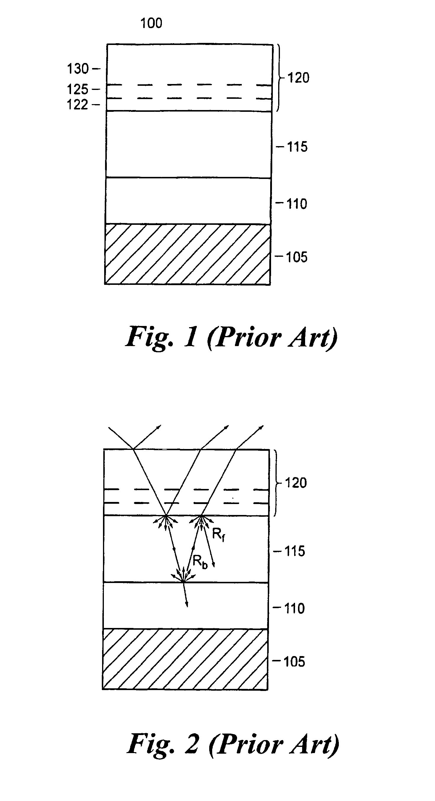
However, given the standard glass / Mo / CIGS / CdS / ZnO / ZnO:Al structure, illustrated in FIG. 1, there is a clear decrease in efficiency compared to devices with thick (˜1.8 μm) absorbers.
This drop in efficiency is mainly due to a reduced short circuit current of the cell due to reduced absorption in the thinner absorbers [2].
Such reflector materials are available, but only overall worse or insignificantly improved power conversion efficiency with respect to devices with the standard Mo back contact has been reported.

Method used


Image

  • Thin Film Solar Cell and Manufacturing Method
  • Thin Film Solar Cell and Manufacturing Method
  • Thin Film Solar Cell and Manufacturing Method

Examples


process examples

[0076]Examples of realization of the above described steps according to the present invention will be described.

Example of Step 615: Formation of the Reflector Layer:

[0077]Zirconium nitride (ZrN) back reflector layers were prepared by reactive DC magnetron sputtering from an elemental Zr target in a mixed argon and nitrogen atmosphere on glass or Mo coated glass substrates. The plasma current was kept constant at 2.5 A in all depositions. Several ZrN deposition series were made, in which the sputter parameters process pressure, argon flow and nitrogen flow were varied. Films with good optical properties were obtained for instance with a process pressure of 5 mTorr, 100 sccm Ar flow, 18 sccm N2 flow, and 400 s deposition time. With these settings, a growth rate of about 2.5 nm / s and a resistivity of 0.45 μΩm was obtained on glass substrates, which for a 400 s deposition leads to a sheet resistance below 0.5 Ω / sq. The growth rate was slightly higher, about 3 nm / s, on Mo substrates.

[00...


PUM


Abstract

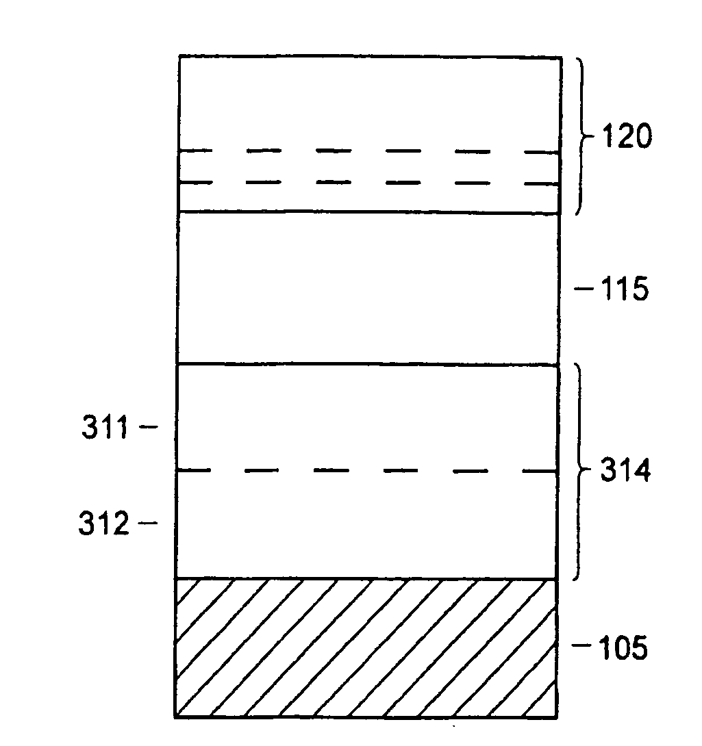
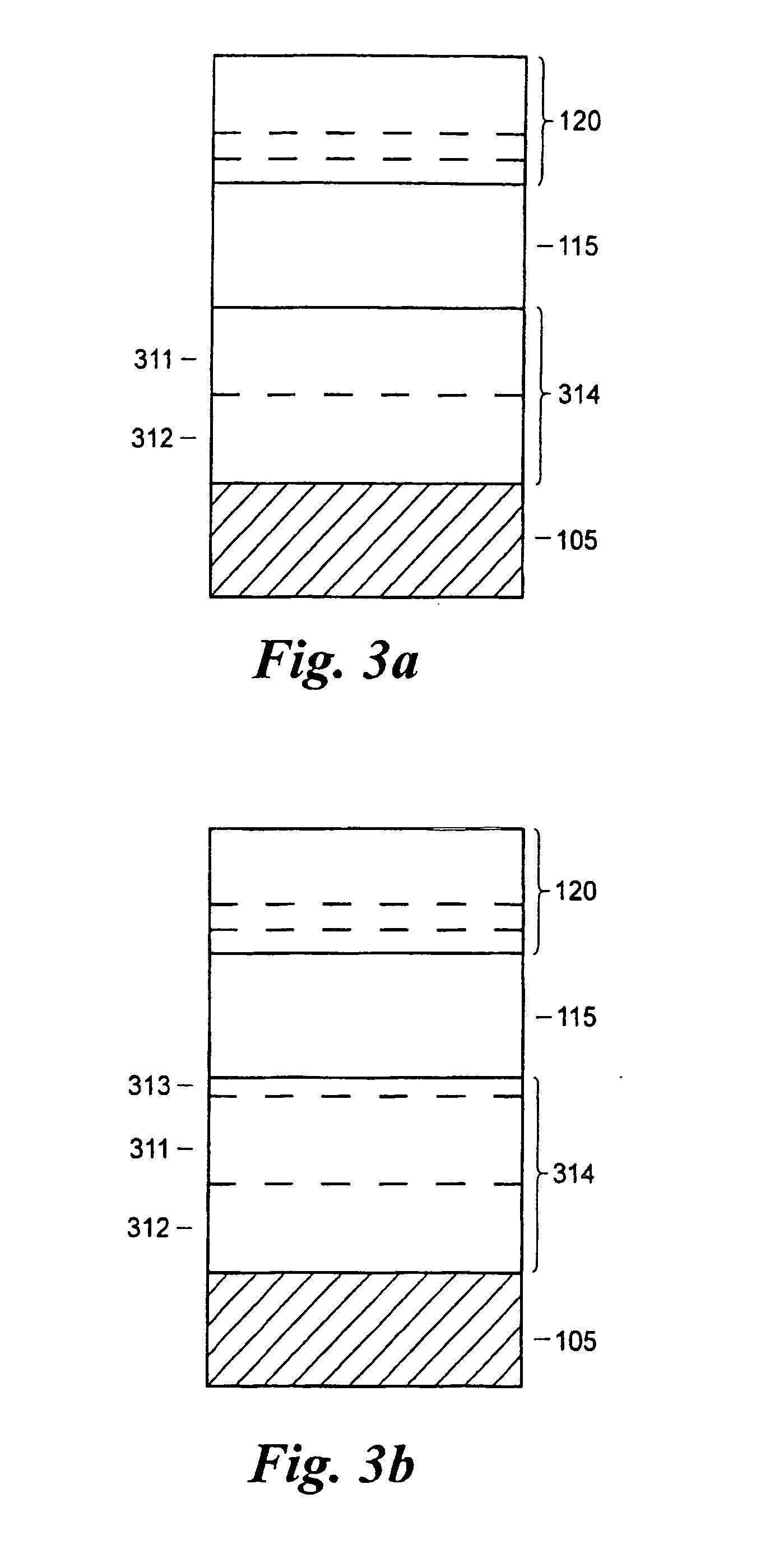
The present invention relates to a thin film solar cell and a method of manufacturing such cells. In particular the invention relates to the use of a composite back contact (314) in Cu(In,Ga)Se2 (CIGS) based thin film solar cells with thin absorber layers. The composite back contact (314) is provided between the substrate (105) and the absorber (115) and comprises: a back reflector layer (311) that enhance the reflectance at the absorber / composite back contact interface; and at least a contact layer that contact layer (310, 313) that ensures suitable electrical properties of the back contact with respect to the absorber; and / or a conductance layer (312) that ensures low sheet resistance for the in-plane current flow.

Description

FIELD OF THE INVENTION[0001]The present invention relates to a thin film solar cell and a method of manufacturing such cells. In particular the invention relates to the use of a back reflector in Cu(In,Ga)Se2 (CIGS) based thin film solar cells with thin absorber layers.BACKGROUND OF THE INVENTION[0002]Solar cells provide a means to produce electrical power with minimal environmental impact since the solar cells directly convert the energy in the solar radiation into electricity. The solar cell, or photovoltaic (PV), technology has shown an substantial development over the recent year, both with regards to the efficiency of the cells, their reliability, useful life and the cost of production. The solar cell technology is now well established and the global market has shown high growth rates of 20-25% p.a. for more than a decade. However, the high cost of PV electricity is still limiting the accessible market.[0003]The Cu(In,Ga)Se2 (CIGS) thin film solar cell technology is considered ...

Claims


Application Information

Patent Timeline
Patent Type & Authority Applications(United States)
IPC IPC(8): H01L31/0248H01L31/0272H01L31/18H01LH01L31/0224H01L31/032H01L31/042H01L31/052
CPCH01L31/022425H01L31/0322H01L31/056Y02E10/541Y02E10/52Y02P70/50
Inventor MALMSTROM, JONASSTOLT, LARS
Owner SOLIBRO RES AB
Learn More